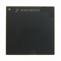
MC68EC060RC50 Freescale Semiconductor, MC68EC060RC50 Datasheet - Page 246

MC68EC060RC50
Manufacturer Part Number
MC68EC060RC50
Description
IC MPU 32BIT 50MHZ 206-PGA
Manufacturer
Freescale Semiconductor
Specifications of MC68EC060RC50
Processor Type
M680x0 32-Bit
Speed
50MHz
Voltage
3.3V
Mounting Type
Surface Mount
Package / Case
206-PGA
Family Name
M68000
Device Core
ColdFire
Device Core Size
32b
Frequency (max)
50MHz
Instruction Set Architecture
RISC
Supply Voltage 1 (typ)
3.3V
Operating Supply Voltage (max)
3.465V
Operating Supply Voltage (min)
3.135V
Operating Temp Range
0C to 110C
Operating Temperature Classification
Commercial
Mounting
Through Hole
Pin Count
206
Package Type
PGA
Lead Free Status / RoHS Status
Contains lead / RoHS non-compliant
Features
-
Lead Free Status / Rohs Status
Compliant
Available stocks
Company
Part Number
Manufacturer
Quantity
Price
Company:
Part Number:
MC68EC060RC50
Manufacturer:
NXP
Quantity:
1 746
- Current page: 246 of 416
- Download datasheet (2Mb)
Exception Processing
interrupting device using an interrupt acknowledge bus cycle with the interrupt level number
output on the transfer modifier signals. For a device that cannot supply an interrupt vector,
the autovector signal (AVEC) must be asserted. In this case, the MC68060 uses an inter-
nally generated autovector, which is one of vector numbers 25–31, that corresponds to the
interrupt level number (see Table 8-1). If external logic indicates a bus error during the inter-
rupt acknowledge cycle, the interrupt is considered spurious, and the processor generates
the spurious interrupt vector number, 24.
Once the vector number is obtained, the processor creates a stack frame of type 0. In this
stack frame, the processor saves the exception vector offset, PC value, and the internal
copy of the SR on the supervisor stack. The saved value of the PC is the logical address of
the next instruction had the interrupt not occurred.
Unlike previous processors of the M68000 family, the MC68060 defers interrupt sampling
from the beginning of exception processing of any exception, up to and until the first instruc-
tion of the exception handler. This allows the first instruction of any exception handler to
raise the interrupt mask level and therefore execute the exception handler without interrupts
(except level 7 interrupts).
Most M68000 family peripherals use programmable interrupt vector numbers as part of the
interrupt acknowledge operation for the system. If this vector number is not initialized after
reset and the peripheral must acknowledge an interrupt request, the peripheral usually
returns the vector number for the uninitialized interrupt vector, 15.
8.2.10 Reset Exception
Asserting the reset in (RSTI) input signal causes a reset exception. The reset exception has
the highest priority of any exception; it provides for system initialization and recovery from
catastrophic failure. Reset also aborts any processing in progress when RSTI is recognized;
processing cannot be recovered. Figure 8-5 is a flowchart of the reset exception processing.
The reset exception places the processor the supervisor mode by setting the S-bit and dis-
ables tracing by clearing the T-bit in the SR. This exception also sets the processor’s inter-
rupt priority mask in the SR to the highest level, level 7. Next the VBR is initialized to zero
($00000000), and all bits in the cache control register (CACR) for the on-chip caches are
cleared. The reset exception also clears the translation control register (TCR). It clears the
enable bit in each of the four transparent translation registers (TTRs). It also clears the bus
control register (BUSCR), and the PCR. The reset also affects the FPU. A quiet not-a-num-
ber (NAN) is loaded into each of the seven floating-point registers, and the floating-point
control register (FPCR), floating-point status register (FPSR), and floating-point instruction
address register (FPIAR) are cleared. If the processor is granted the bus, and the processor
does not detect TS asserted (possibly by an alternate master), the processor then performs
two long-word read bus cycles. The first long word, at address 0, is loaded into the SP, and
the second long word, at address 4, is loaded into the PC. Reset exception processing con-
cludes with the transfer of control to the memory location defined by the PC.
After the initial instruction is fetched, program execution begins at the address in the PC.
The reset exception does not flush the ATCs or invalidate entries in the instruction or data
caches; it does not save the value of either the PC or the SR. If an access error or address
8-14
M68060 USER’S MANUAL
MOTOROLA
Related parts for MC68EC060RC50
Image
Part Number
Description
Manufacturer
Datasheet
Request
R
Part Number:
Description:
Manufacturer:
Freescale Semiconductor, Inc
Datasheet:
Part Number:
Description:
Manufacturer:
Freescale Semiconductor, Inc
Datasheet:
Part Number:
Description:
Manufacturer:
Freescale Semiconductor, Inc
Datasheet:
Part Number:
Description:
Manufacturer:
Freescale Semiconductor, Inc
Datasheet:
Part Number:
Description:
Manufacturer:
Freescale Semiconductor, Inc
Datasheet:
Part Number:
Description:
Manufacturer:
Freescale Semiconductor, Inc
Datasheet:
Part Number:
Description:
Manufacturer:
Freescale Semiconductor, Inc
Datasheet:
Part Number:
Description:
Manufacturer:
Freescale Semiconductor, Inc
Datasheet:
Part Number:
Description:
Manufacturer:
Freescale Semiconductor, Inc
Datasheet:
Part Number:
Description:
Manufacturer:
Freescale Semiconductor, Inc
Datasheet:
Part Number:
Description:
Manufacturer:
Freescale Semiconductor, Inc
Datasheet:
Part Number:
Description:
Manufacturer:
Freescale Semiconductor, Inc
Datasheet:
Part Number:
Description:
Manufacturer:
Freescale Semiconductor, Inc
Datasheet:
Part Number:
Description:
Manufacturer:
Freescale Semiconductor, Inc
Datasheet:
Part Number:
Description:
Manufacturer:
Freescale Semiconductor, Inc
Datasheet:


