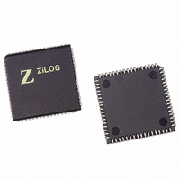
Z16C3516VSG Zilog, Z16C3516VSG Datasheet - Page 15

Z16C3516VSG
Manufacturer Part Number
Z16C3516VSG
Description
IC 16MHZ Z8500 CMOS ISCC 68-PLCC
Manufacturer
Zilog
Series
IUSC™r
Specifications of Z16C3516VSG
Controller Type
Serial Communications Controller (SCC)
Interface
USB
Voltage - Supply
4.75 V ~ 5.25 V
Current - Supply
50mA
Operating Temperature
0°C ~ 70°C
Mounting Type
Surface Mount
Package / Case
68-LCC (J-Lead)
Lead Free Status / RoHS Status
Lead free / RoHS Compliant
Other names
269-4690-5
Z16C3516VSG
Z16C3516VSG
Available stocks
Company
Part Number
Manufacturer
Quantity
Price
Company:
Part Number:
Z16C3516VSG
Manufacturer:
INTEL
Quantity:
6 219
- Current page: 15 of 268
- Download datasheet (3Mb)
UM011001-0601
2.4 REGISTER ACCESS
ISCC registers may be accessed explicitly, directly or indi-
rectly. Explicit addressing occurs only for three registers in
the ISCC: these are the Bus Configuration Register (for the
first write after a hardware reset), the RDR (Receive Data
Register) by a fly-by DMA read, and the TDR (Transmit
Data Register) by a fly-by DMA write. In the non-multi-
plexed bus case, only WR0/RR0 of the SCC cell and only
the Channel Command/Address Register of the DMA cell
are accessed directly. Other registers are accessed using
the pointers in these directly accessed registers. In the
multiplexed bus case, all registers (except the WR0, RR0
and CCAR) are accessed through a two step ad-
dress/read-write bus transaction. In this case there are two
options available for address decoding: shift right and shift
left. These options are independently selectable for both
the SCC cell and the DMA cell.
2.4.1 SCC Cell Register Access,
Multiplexed Bus
The registers in the ISCC in the multiplexed bus mode are
addressed via the address on AD7-AD0 which is latched
by the rising edge of /AS. As discussed in the paragraphs
below, the address contains a bit to select the SCC cell
channel (A or B). Although this selection is in the address,
the A1/A//B input remains active and must be set to select
Channel A for the selection bit in the AD7-AD0 address to
function correctly. Conversely, the A1/A//B pin may also be
used to select the channel instead of the bit in the AD7-
AD0 address. In this case, the bit in the AD7-AD0 address
must be set to select Channel A for the A1/A//B input to
function correctly.
There are two address decoding modes: shift left and shift
right. In shift left mode, the register address is decoded
from AD5-AD1. This mode is set by a hardware reset.
In the shift left mode, the register address itself is placed on
AD4-AD1 and the Channel Select bit, A/B, is decoded from
AD5. The register map for this case is shown in Table 2-2.
Address
AD5-AD1
10000
10001
10010
10011
10100
10101
10110
10111
11000
11001
11010
11011
11100
11101
11110
11111
Note: The above table applies to Channel “B” also.
In Shift Right Mode, bits 0-1 in WR0A controls which bits
will be decoded to form the register address. It is placed in
this register to simplify programming when the current
state of the Shift Right/Shift Left bit is not known.
The register address is decoded from AD4-AD0. The Shift
Right/Shift Left bit is written via command to make the soft-
ware writing to WR0 independent of the state of the Shift
Right/Shift Left bit.
AD4-AD0 is the actual register address and AD0 deter-
mines the channel selection (A//B). The register map is
shown in Table 2-3.
Because the ISCC SCC Cell does not contain 16 read reg-
isters, the decoding of the read registers is not complete;
this is indicated in Table 2-2 and Table 2-3 by parentheses
around the register name. These addresses may also be
used to access the read registers.
Note also that in the multiplexed bus mode, only one WR2
and WR9 are shown in the address map; these registers
may be written from either SCC cell channel.
Table 2-2. SCC Cell Address Map,
Multiplexed Bus Mode, Shift Left
Write
WR0A
WR1A
WR2
WR3A
WR4A
WR5A
WR6A
WR7A
WR8A
WR9
WR10A
WR11A
WR12A
WR13A
WR14A
WR15A
Z16C35 ISCC™ User’s Manual
Interfacing the ISCC™
Read
RR0A
RR1A
RR2A
RR3A
(RR0A)
(RR1A)
(RR2A)
(RR3A)
RR8A
(RR13A)
RR10A
(RR15A)
RR12A
RR13A
(RR10A)
RR15A
2-5
2
Related parts for Z16C3516VSG
Image
Part Number
Description
Manufacturer
Datasheet
Request
R

Part Number:
Description:
CMOS ISCC INTEGRATED SERIAL COMMUNICATIONS CONTROLLER
Manufacturer:
ZILOG [Zilog, Inc.]
Datasheet:

Part Number:
Description:
Communication Controllers, ZILOG INTELLIGENT PERIPHERAL CONTROLLER (ZIP)
Manufacturer:
Zilog, Inc.
Datasheet:

Part Number:
Description:
KIT DEV FOR Z8 ENCORE 16K TO 64K
Manufacturer:
Zilog
Datasheet:

Part Number:
Description:
KIT DEV Z8 ENCORE XP 28-PIN
Manufacturer:
Zilog
Datasheet:

Part Number:
Description:
DEV KIT FOR Z8 ENCORE 8K/4K
Manufacturer:
Zilog
Datasheet:

Part Number:
Description:
KIT DEV Z8 ENCORE XP 28-PIN
Manufacturer:
Zilog
Datasheet:

Part Number:
Description:
DEV KIT FOR Z8 ENCORE 4K TO 8K
Manufacturer:
Zilog
Datasheet:

Part Number:
Description:
CMOS Z8 microcontroller. ROM 16 Kbytes, RAM 256 bytes, speed 16 MHz, 32 lines I/O, 3.0V to 5.5V
Manufacturer:
Zilog, Inc.
Datasheet:

Part Number:
Description:
Low-cost microcontroller. 512 bytes ROM, 61 bytes RAM, 8 MHz
Manufacturer:
Zilog, Inc.
Datasheet:

Part Number:
Description:
Z8 4K OTP Microcontroller
Manufacturer:
Zilog, Inc.
Datasheet:

Part Number:
Description:
CMOS SUPER8 ROMLESS MCU
Manufacturer:
Zilog, Inc.
Datasheet:

Part Number:
Description:
SL1866 CMOSZ8 OTP Microcontroller
Manufacturer:
Zilog, Inc.
Datasheet:

Part Number:
Description:
SL1866 CMOSZ8 OTP Microcontroller
Manufacturer:
Zilog, Inc.
Datasheet:

Part Number:
Description:
OTP (KB) = 1, RAM = 125, Speed = 12, I/O = 14, 8-bit Timers = 2, Comm Interfaces Other Features = Por, LV Protect, Voltage = 4.5-5.5V
Manufacturer:
Zilog, Inc.
Datasheet:


