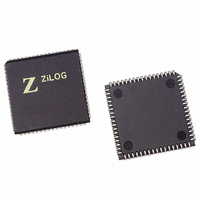
Z16C3516VSG Zilog, Z16C3516VSG Datasheet - Page 62

Z16C3516VSG
Manufacturer Part Number
Z16C3516VSG
Description
IC 16MHZ Z8500 CMOS ISCC 68-PLCC
Manufacturer
Zilog
Series
IUSC™r
Specifications of Z16C3516VSG
Controller Type
Serial Communications Controller (SCC)
Interface
USB
Voltage - Supply
4.75 V ~ 5.25 V
Current - Supply
50mA
Operating Temperature
0°C ~ 70°C
Mounting Type
Surface Mount
Package / Case
68-LCC (J-Lead)
Lead Free Status / RoHS Status
Lead free / RoHS Compliant
Other names
269-4690-5
Z16C3516VSG
Z16C3516VSG
Available stocks
Company
Part Number
Manufacturer
Quantity
Price
Company:
Part Number:
Z16C3516VSG
Manufacturer:
INTEL
Quantity:
6 219
- Current page: 62 of 268
- Download datasheet (3Mb)
Z16C35ISCC™ User’s Manual
Register Descriptions
5.2 REGISTER DESCRIPTIONS (Continued)
5.2.2 Read Registers, SCC Cell
Four read registers indicate status information, two are for
baud rate generation, and one for the receive buffer. In ad-
dition, there are two read registers which are shared by
both channels: one for the interrupt pending bits and one
for interrupt vector. See Table 5-2 for a summary on the
SCC cell read registers.
Register
RR0
RR1
RR2
RR3
RR6
RR7
RR8
RR10
RR12
RR13
RR15
5.2.3 DMA Registers
The DMA cell contains 16 read write registers for con-
trol of the DMA channels. The DMA possesses its own
interrupt vector register and interrupt control registers
which are independent of the SCC cell. The DMA cell
also includes the Bus Configuration Register (BCR) for
5.3 SCC CELL REGISTER OVERVIEW
The SCC cell write register set in each channel includes
ten control registers (among them is the transmit buffer),
two sync character registers and two baud rate time con-
stant registers. The interrupt control register and the mas-
ter interrupt control and reset register are shared by both
channels.
5-2
Table 5-2. SCC Cell Read Registers
Description
Transmit and Receive buffer status and
external status
Special Receive Condition status
Modified interrupt vector (Channel B only),
Unmodified
interrupt vector (Channel A only)
Interrupt pending bits (Channel A only)
SDLC FIFO byte counter lower byte (only
when enabled)
SDLC FIFO byte count and status (only when
enabled)
Receive buffer
Miscellaneous status bits
Lower byte of baud rate generator time
constant
Upper byte of baud rate generator time
constant
External Status interrupt information
P R E L I M I N A R Y
the ISCC. The addresses, names and descriptions of
these registers are given in Table 5-3.
Address
xxxxx
00000
00000
00001
00010
00011
00011
00100
00101
00110
00111
01000-01001 RDCRA Receive DMA Count Register
01010-01011 TDCRA Transmit DMA Count Register
01100-01101 RDCRB Receive DMA Count Register
01110-01111 TDCRB Transmit DMA Count Register
10000-10011 RDARA Receive DMA Address Register
10100-10111 TDARA Transmit DMA Address Register
11000-11011 RDARB Receive DMA Address Register
11100-11111 TDARB Transmit DMA Address Register
The only variation in register definition is between the mul-
tiplexed and non-multiplexed bus mode programming of
the ISCC. The variation exists in the command decode
structure; register WR0. The following sections describe in
detail each write register and the associated bit configura-
tion for each.
Table 5-3. DMA Cell Register Description
Name
BCR
CCAR
DSR
ICR
IVR
ICSR
ISR
DER
DCR
Description
Bus Configuration Register
Channel Command/Address
Register (Write)
DMA Status Register (Read)
Interrupt Control Register
Interrupt Vector Register
Interrupt Command Register
(Write)
Interrupt Status Register (Read)
DMA Enable/Disable Register
DMA Control Register
Reserved Address
Reserved Address
Channel A (Low-high byte)
Channel A
Channel B
Channel B
Channel A
Channel A
Channel B
Channel B
UM011001-0601
Related parts for Z16C3516VSG
Image
Part Number
Description
Manufacturer
Datasheet
Request
R

Part Number:
Description:
CMOS ISCC INTEGRATED SERIAL COMMUNICATIONS CONTROLLER
Manufacturer:
ZILOG [Zilog, Inc.]
Datasheet:

Part Number:
Description:
Communication Controllers, ZILOG INTELLIGENT PERIPHERAL CONTROLLER (ZIP)
Manufacturer:
Zilog, Inc.
Datasheet:

Part Number:
Description:
KIT DEV FOR Z8 ENCORE 16K TO 64K
Manufacturer:
Zilog
Datasheet:

Part Number:
Description:
KIT DEV Z8 ENCORE XP 28-PIN
Manufacturer:
Zilog
Datasheet:

Part Number:
Description:
DEV KIT FOR Z8 ENCORE 8K/4K
Manufacturer:
Zilog
Datasheet:

Part Number:
Description:
KIT DEV Z8 ENCORE XP 28-PIN
Manufacturer:
Zilog
Datasheet:

Part Number:
Description:
DEV KIT FOR Z8 ENCORE 4K TO 8K
Manufacturer:
Zilog
Datasheet:

Part Number:
Description:
CMOS Z8 microcontroller. ROM 16 Kbytes, RAM 256 bytes, speed 16 MHz, 32 lines I/O, 3.0V to 5.5V
Manufacturer:
Zilog, Inc.
Datasheet:

Part Number:
Description:
Low-cost microcontroller. 512 bytes ROM, 61 bytes RAM, 8 MHz
Manufacturer:
Zilog, Inc.
Datasheet:

Part Number:
Description:
Z8 4K OTP Microcontroller
Manufacturer:
Zilog, Inc.
Datasheet:

Part Number:
Description:
CMOS SUPER8 ROMLESS MCU
Manufacturer:
Zilog, Inc.
Datasheet:

Part Number:
Description:
SL1866 CMOSZ8 OTP Microcontroller
Manufacturer:
Zilog, Inc.
Datasheet:

Part Number:
Description:
SL1866 CMOSZ8 OTP Microcontroller
Manufacturer:
Zilog, Inc.
Datasheet:

Part Number:
Description:
OTP (KB) = 1, RAM = 125, Speed = 12, I/O = 14, 8-bit Timers = 2, Comm Interfaces Other Features = Por, LV Protect, Voltage = 4.5-5.5V
Manufacturer:
Zilog, Inc.
Datasheet:


