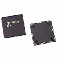
Z16C3516VSG Zilog, Z16C3516VSG Datasheet - Page 163

Z16C3516VSG
Manufacturer Part Number
Z16C3516VSG
Description
IC 16MHZ Z8500 CMOS ISCC 68-PLCC
Manufacturer
Zilog
Series
IUSC™r
Specifications of Z16C3516VSG
Controller Type
Serial Communications Controller (SCC)
Interface
USB
Voltage - Supply
4.75 V ~ 5.25 V
Current - Supply
50mA
Operating Temperature
0°C ~ 70°C
Mounting Type
Surface Mount
Package / Case
68-LCC (J-Lead)
Lead Free Status / RoHS Status
Lead free / RoHS Compliant
Other names
269-4690-5
Z16C3516VSG
Z16C3516VSG
Available stocks
Company
Part Number
Manufacturer
Quantity
Price
Company:
Part Number:
Z16C3516VSG
Manufacturer:
INTEL
Quantity:
6 219
- Current page: 163 of 268
- Download datasheet (3Mb)
UM011001-0601
Note: To maximize compatibility, program an MUSC using the second half of this range, (PBA)+384 through (PBA)+511.
While the ESCC and ISCC can drive their Baud Rate
Generators from their PCLK inputs, the (M)USC has no
such input. The 80186 clock output SYSCLK is brought to
IUSC
Since
addresses and data on the AD lines, the IUSC is
configured to use these addresses. Software need not
write register addresses into the indirect address fields of
the IUSC’s CCAR and DCAR.
The IUSC’s two DMA channels allow its Receiver and
Transmitter to be handled on a polled, interrupt-driven, or
DMA basis, in any combination.
The IUSC can be programmed using 16-bit data on the
AD15-AD0 lines or 8-bit data on AD15-AD8 and AD7-AD0.
The distinction between 8-bit and 16-bit operations is
made as part of the address map rather than via a control
input. The D//C pin of the IUSC is driven from A7 during
slave cycles, and the S//D pin is driven from A8. The
overall address range of the IUSC is 384 bytes from
(PBA)+512 through (PBA)+895.
The first write to this address range, after a Reset,
implicitly writes the IUSC’s Bus Configuration Register
(BCR). To match up with the rest of the board’s hardware,
this first write is a 16-bit write, storing the recommended
hex value 00F7 at any word address in the range
(PBA)+768 through (PBA)+830. Details of this transaction
are as follows:
The High on the IUSC’s S//D input, which is connected
to A8, selects the WAIT protocol on the /WAIT//RDY pin,
which is how the 80186 works.
It may not be required for this initial write, but it is good
programming form for A6 to be zero since this is a word
write. This and the previous point determine the
recommended address range.
The MSB of the data (D15) is 0 because a separate non-
multiplexed address is not wired to pins AD13:8 of the
IUSC.
Bits 14-8 are more or less required to be all 0 by the
IUSC’s internal logic.
Starting Addr
(PBA)+256
(PBA)+320
(PBA)+384
(PBA)+448
the
80186
processor
Ending Addr
(PBA)+319
(PBA)+383
(PBA)+447
(PBA)+511
provides
multiplexed
pins 7 of J9, J10, and J12, at which point it can be
jumpered to pin 9 or 8 so that it is routed to the /TxC or
/RxC pin of the device.
Given that the BCR is written as above, the IUSC slave-
mode address map is as follows:
Registers Accessed
16-bit access to MUSC regs or USC channel B regs
8-bit access to MUSC regs or USC channel B regs
16-bit access to MUSC regs or USC channel A regs
8-bit access to MUSC regs or USC channel A regs
D7-D6 are 11 to allow the DMA controllers to do either
16-bit transfers, or alternating byte transfers on AD7-
AD0 for even-addressed bytes and on AD15-AD8 for
odd-addressed bytes. This is compatible with 80186
byte ordering.
D5-D4 of the data are 11 to select double-pulsed mode
for the IUSC’s /INTACK input. Again, this is how the
80186 works.
D3 of the data is 0 to select open-drain mode on the
IUSC’s /BUSREQ pin. The board’s control logic also
drives this signal low when the ISCC asserts its Bus
Request output.
D2 of the data is 1 to tell the IUSC that the data bus is 16
bits wide.
D1 of the data is 1 to select open-drain mode on the
IUSC’s /INT pin which is OR-tied with the interrupt
request from the (E)SCC.
D0 of the data is 1 to select Shift Right Address mode,
so that the IUSC subsequently takes register addressing
from the AD6-AD0 lines rather than from AD7-AD1.
The fact that the IUSC’s internal logic sees activity on its
/AS pin, which is inverted from the 80186' ALE signal,
automatically
Address/Data bus.
The Zilog Datacom Family with the 80186 CPU
conditions
it
for
Application Note
a
multiplexed
9-9
8
Related parts for Z16C3516VSG
Image
Part Number
Description
Manufacturer
Datasheet
Request
R

Part Number:
Description:
CMOS ISCC INTEGRATED SERIAL COMMUNICATIONS CONTROLLER
Manufacturer:
ZILOG [Zilog, Inc.]
Datasheet:

Part Number:
Description:
Communication Controllers, ZILOG INTELLIGENT PERIPHERAL CONTROLLER (ZIP)
Manufacturer:
Zilog, Inc.
Datasheet:

Part Number:
Description:
KIT DEV FOR Z8 ENCORE 16K TO 64K
Manufacturer:
Zilog
Datasheet:

Part Number:
Description:
KIT DEV Z8 ENCORE XP 28-PIN
Manufacturer:
Zilog
Datasheet:

Part Number:
Description:
DEV KIT FOR Z8 ENCORE 8K/4K
Manufacturer:
Zilog
Datasheet:

Part Number:
Description:
KIT DEV Z8 ENCORE XP 28-PIN
Manufacturer:
Zilog
Datasheet:

Part Number:
Description:
DEV KIT FOR Z8 ENCORE 4K TO 8K
Manufacturer:
Zilog
Datasheet:

Part Number:
Description:
CMOS Z8 microcontroller. ROM 16 Kbytes, RAM 256 bytes, speed 16 MHz, 32 lines I/O, 3.0V to 5.5V
Manufacturer:
Zilog, Inc.
Datasheet:

Part Number:
Description:
Low-cost microcontroller. 512 bytes ROM, 61 bytes RAM, 8 MHz
Manufacturer:
Zilog, Inc.
Datasheet:

Part Number:
Description:
Z8 4K OTP Microcontroller
Manufacturer:
Zilog, Inc.
Datasheet:

Part Number:
Description:
CMOS SUPER8 ROMLESS MCU
Manufacturer:
Zilog, Inc.
Datasheet:

Part Number:
Description:
SL1866 CMOSZ8 OTP Microcontroller
Manufacturer:
Zilog, Inc.
Datasheet:

Part Number:
Description:
SL1866 CMOSZ8 OTP Microcontroller
Manufacturer:
Zilog, Inc.
Datasheet:

Part Number:
Description:
OTP (KB) = 1, RAM = 125, Speed = 12, I/O = 14, 8-bit Timers = 2, Comm Interfaces Other Features = Por, LV Protect, Voltage = 4.5-5.5V
Manufacturer:
Zilog, Inc.
Datasheet:


