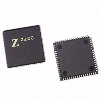
Z16C3516VSG Zilog, Z16C3516VSG Datasheet - Page 61

Z16C3516VSG
Manufacturer Part Number
Z16C3516VSG
Description
IC 16MHZ Z8500 CMOS ISCC 68-PLCC
Manufacturer
Zilog
Series
IUSC™r
Specifications of Z16C3516VSG
Controller Type
Serial Communications Controller (SCC)
Interface
USB
Voltage - Supply
4.75 V ~ 5.25 V
Current - Supply
50mA
Operating Temperature
0°C ~ 70°C
Mounting Type
Surface Mount
Package / Case
68-LCC (J-Lead)
Lead Free Status / RoHS Status
Lead free / RoHS Compliant
Other names
269-4690-5
Z16C3516VSG
Z16C3516VSG
Available stocks
Company
Part Number
Manufacturer
Quantity
Price
Company:
Part Number:
Z16C3516VSG
Manufacturer:
INTEL
Quantity:
6 219
- Current page: 61 of 268
- Download datasheet (3Mb)
5.1 INTRODUCTION
This section describes the function of the various bits in the
registers of the device. Throughout this section the follow-
ing conventions will be used:
Control bits may be written and read by the CPU and will
not be modified by the device. Command bits may be writ-
ten by the CPU to initiate an action in the device and will be
read as zeros. Status bits are controlled by the device and
may be read to check device status. Any writes to status
bits are ignored by the device. Command/status bits are
controlled by both the device and the CPU. They may be
5.2 REGISTER DESCRIPTIONS
Register can be accessed through either channel, the In-
terrupt Vector Read Register returns the interrupt vector
with status if read from Channel B and without status if
read from Channel A, and Channel A has an additional
read register which contains all the Interrupt Pending bits.
5.2.1 Write Registers, SCC Cell
Ten write registers are used for control, two for sync char-
acter generation, and two for baud rate generation. In ad-
dition, there are two write registers which are shared by
both channels; one is the interrupt vector register, and one
is the master interrupt control and reset register. See Table
5-1 for a summary on write registers.
UM011001-0601
P R E L I M I N A R Y
U
C
R
written and read by the CPU and may also be modified by
the device.
Reserved bits are not used in this implementation of the
device and may or may not be physically present in the de-
vice. Reserved bits that are physically present will be read-
able and writable but reserved bits that are not present will
always be read as zero. To ensure compatibility with future
versions of the device reserved bits should always be writ-
ten with zeros. Reserved commands should not be used
for the same reason.
Register
WR0
WR1
WR2
WR3
WR4
WR5
WR6
WR7
WR8
WR9
WR10
WR11
WR12
WR13
WR14
WR15
SER
EGISTER
HAPTER
’
S
M
Table 5-1. SCC Cell Write Registers
Description
Register Pointers, various initialization
commands
Transmit and Receive interrupt enables,
commands WAIT/DMA
Interrupt Vector
Receive parameters and control modes
Transmit and Receive modes and parameters
Transmit parameters and control modes
Sync Character or SDLC address
Sync Character or SDLC flag
Transmit buffer
Master Interrupt control and reset commands
Misc. transmit and receive control bits
Clock mode controls for receive and transmit
Lower byte of baud rate generator
Upper byte of baud rate generator
Miscellaneous control bits
External status interrupt enable control
ANUAL
D
ESCRIPTIONS
5
5-1
5
Related parts for Z16C3516VSG
Image
Part Number
Description
Manufacturer
Datasheet
Request
R

Part Number:
Description:
CMOS ISCC INTEGRATED SERIAL COMMUNICATIONS CONTROLLER
Manufacturer:
ZILOG [Zilog, Inc.]
Datasheet:

Part Number:
Description:
Communication Controllers, ZILOG INTELLIGENT PERIPHERAL CONTROLLER (ZIP)
Manufacturer:
Zilog, Inc.
Datasheet:

Part Number:
Description:
KIT DEV FOR Z8 ENCORE 16K TO 64K
Manufacturer:
Zilog
Datasheet:

Part Number:
Description:
KIT DEV Z8 ENCORE XP 28-PIN
Manufacturer:
Zilog
Datasheet:

Part Number:
Description:
DEV KIT FOR Z8 ENCORE 8K/4K
Manufacturer:
Zilog
Datasheet:

Part Number:
Description:
KIT DEV Z8 ENCORE XP 28-PIN
Manufacturer:
Zilog
Datasheet:

Part Number:
Description:
DEV KIT FOR Z8 ENCORE 4K TO 8K
Manufacturer:
Zilog
Datasheet:

Part Number:
Description:
CMOS Z8 microcontroller. ROM 16 Kbytes, RAM 256 bytes, speed 16 MHz, 32 lines I/O, 3.0V to 5.5V
Manufacturer:
Zilog, Inc.
Datasheet:

Part Number:
Description:
Low-cost microcontroller. 512 bytes ROM, 61 bytes RAM, 8 MHz
Manufacturer:
Zilog, Inc.
Datasheet:

Part Number:
Description:
Z8 4K OTP Microcontroller
Manufacturer:
Zilog, Inc.
Datasheet:

Part Number:
Description:
CMOS SUPER8 ROMLESS MCU
Manufacturer:
Zilog, Inc.
Datasheet:

Part Number:
Description:
SL1866 CMOSZ8 OTP Microcontroller
Manufacturer:
Zilog, Inc.
Datasheet:

Part Number:
Description:
SL1866 CMOSZ8 OTP Microcontroller
Manufacturer:
Zilog, Inc.
Datasheet:

Part Number:
Description:
OTP (KB) = 1, RAM = 125, Speed = 12, I/O = 14, 8-bit Timers = 2, Comm Interfaces Other Features = Por, LV Protect, Voltage = 4.5-5.5V
Manufacturer:
Zilog, Inc.
Datasheet:


