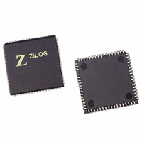
Z16C3516VSG Zilog, Z16C3516VSG Datasheet - Page 96

Z16C3516VSG
Manufacturer Part Number
Z16C3516VSG
Description
IC 16MHZ Z8500 CMOS ISCC 68-PLCC
Manufacturer
Zilog
Series
IUSC™r
Specifications of Z16C3516VSG
Controller Type
Serial Communications Controller (SCC)
Interface
USB
Voltage - Supply
4.75 V ~ 5.25 V
Current - Supply
50mA
Operating Temperature
0°C ~ 70°C
Mounting Type
Surface Mount
Package / Case
68-LCC (J-Lead)
Lead Free Status / RoHS Status
Lead free / RoHS Compliant
Other names
269-4690-5
Z16C3516VSG
Z16C3516VSG
Available stocks
Company
Part Number
Manufacturer
Quantity
Price
Company:
Part Number:
Z16C3516VSG
Manufacturer:
INTEL
Quantity:
6 219
- Current page: 96 of 268
- Download datasheet (3Mb)
Z16C35ISCC™ User’s Manual
Register Descriptions
5.6 DMA CELL REGISTER DESCRIPTIONS (Continued)
5.6.13 Bus Configuration Register
The first write to the ISCC after a hardware reset is always
to the Bus Configuration Register. The register is shown in
Figure 5-38. The Bus Configuration Register is not affect-
ed by any reset function other than a hardware reset and
is accessible only after the hardware reset. Note that when
writing to the Bus Configuration Register, /AS and A1/A//B
are used to program certain bus interface features. Refer
to the Bus Interface Unit description for details.
Bit D7 is the Byte Swap Enable
A zero in this bit disables the byte swap feature. Thus the
ISCC accepts DMA transferred data from memory on the
lower eight bits of the address data bus (AD) and ignores
data on the upper eight bits.
A one in this bit enables the byte swap feature and the
ISCC accepts DMA transferred data from memory on ei-
ther the upper or lower eight bits of the bus depending on
the state of A0, the least significant address bit. Big endian
or little endian selection is made through bit D6.
Note that whether or not this feature is enabled, when
data is DMA transferred from the ISCC to memory, the
ISCC replicates the same data on both the lower and up-
5-36
D7
D6
Figure 5-39. Bus Configuration Register
D5 D4 D3 D2 D1 D0
0
0
1
1
0
1
0
1
Interrupt Acknowledge Type
Status Acknowledge
Pulsed Acknowledge
Reserved
Double-Pulsed Acknowledge
Reserved
Byte Swap Select
Byte Swap Enable
Shift Right/Left Address
for DMA
P R E L I M I N A R Y
per eight bits of the bus. Writing to memory is controlled
by the external generation of appropriate memory enable
or strobe signals.
Bit D6 controls the odd/even byte selection when the Byte
Swap feature is enabled. If Byte Swap Select is a 1, then
even address bytes (transfers where the DMA address
has A0 equal to 0) are accepted by the ISCC on the lower
eight bits of the bus and odd address bytes (transfers
where the DMA address has A0 equal to 1) are accepted
on the upper eight bits of the bus. If Byte Swap Select is a
0, then even address bytes (transfers where the DMA ad-
dress has A0 equal to 0) are accepted by the ISCC on the
upper eight bits of the bus and odd address bytes (trans-
fers where the DMA address has A0 equal to 1) are ac-
cepted on the lower eight bits of the bus.
Bits D5 through D3 are reserved and should be pro-
grammed zero.
Bits D2 and D1 program the Interrupt acknowledge type
according to Table 5-16.
The Status Acknowledge is compatible with the 68000 fam-
ily of microprocessors and the Double Pulse Acknowledge
is compatible withe the 8086 family or microprocessors.
Bit D0 selects the Shift Right/Shift Left address decoding
mode for the DMA cell only. A 1 in this bit selects the Shift
Right mode. In this mode, when the ISCC is in the multi-
plexed bus mode, the addresses to the DMA cell registers
is decoded from address data lines AD4 through AD0. A 0
in this bit selects the Shift Left mode. In this mode, when
the ISCC is in the multiplexed bus mode, the addresses to
the DMA cell registers is decoded from address data lines
AD5 through AD1.
Table 5-16. Interrupt Acknowledge Programming
D2
0
0
1
1
D1
0
1
0
1
Interrupt Acknowledge Type
Status Acknowledge
Pulsed Acknowledge
Reserved
Double Pulse Acknowledge
UM011001-0601
Related parts for Z16C3516VSG
Image
Part Number
Description
Manufacturer
Datasheet
Request
R

Part Number:
Description:
CMOS ISCC INTEGRATED SERIAL COMMUNICATIONS CONTROLLER
Manufacturer:
ZILOG [Zilog, Inc.]
Datasheet:

Part Number:
Description:
Communication Controllers, ZILOG INTELLIGENT PERIPHERAL CONTROLLER (ZIP)
Manufacturer:
Zilog, Inc.
Datasheet:

Part Number:
Description:
KIT DEV FOR Z8 ENCORE 16K TO 64K
Manufacturer:
Zilog
Datasheet:

Part Number:
Description:
KIT DEV Z8 ENCORE XP 28-PIN
Manufacturer:
Zilog
Datasheet:

Part Number:
Description:
DEV KIT FOR Z8 ENCORE 8K/4K
Manufacturer:
Zilog
Datasheet:

Part Number:
Description:
KIT DEV Z8 ENCORE XP 28-PIN
Manufacturer:
Zilog
Datasheet:

Part Number:
Description:
DEV KIT FOR Z8 ENCORE 4K TO 8K
Manufacturer:
Zilog
Datasheet:

Part Number:
Description:
CMOS Z8 microcontroller. ROM 16 Kbytes, RAM 256 bytes, speed 16 MHz, 32 lines I/O, 3.0V to 5.5V
Manufacturer:
Zilog, Inc.
Datasheet:

Part Number:
Description:
Low-cost microcontroller. 512 bytes ROM, 61 bytes RAM, 8 MHz
Manufacturer:
Zilog, Inc.
Datasheet:

Part Number:
Description:
Z8 4K OTP Microcontroller
Manufacturer:
Zilog, Inc.
Datasheet:

Part Number:
Description:
CMOS SUPER8 ROMLESS MCU
Manufacturer:
Zilog, Inc.
Datasheet:

Part Number:
Description:
SL1866 CMOSZ8 OTP Microcontroller
Manufacturer:
Zilog, Inc.
Datasheet:

Part Number:
Description:
SL1866 CMOSZ8 OTP Microcontroller
Manufacturer:
Zilog, Inc.
Datasheet:

Part Number:
Description:
OTP (KB) = 1, RAM = 125, Speed = 12, I/O = 14, 8-bit Timers = 2, Comm Interfaces Other Features = Por, LV Protect, Voltage = 4.5-5.5V
Manufacturer:
Zilog, Inc.
Datasheet:


