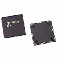
Z16C3516VSG Zilog, Z16C3516VSG Datasheet - Page 34

Z16C3516VSG
Manufacturer Part Number
Z16C3516VSG
Description
IC 16MHZ Z8500 CMOS ISCC 68-PLCC
Manufacturer
Zilog
Series
IUSC™r
Specifications of Z16C3516VSG
Controller Type
Serial Communications Controller (SCC)
Interface
USB
Voltage - Supply
4.75 V ~ 5.25 V
Current - Supply
50mA
Operating Temperature
0°C ~ 70°C
Mounting Type
Surface Mount
Package / Case
68-LCC (J-Lead)
Lead Free Status / RoHS Status
Lead free / RoHS Compliant
Other names
269-4690-5
Z16C3516VSG
Z16C3516VSG
Available stocks
Company
Part Number
Manufacturer
Quantity
Price
Company:
Part Number:
Z16C3516VSG
Manufacturer:
INTEL
Quantity:
6 219
- Current page: 34 of 268
- Download datasheet (3Mb)
Z16C35ISCC™ User’s Manual
ISCC™ DMA and Ancillary Support Circuitry
Figure 3-10 shows three examples of clock sources and
selection. Part (a) of the figure shows the clock set up for
asynchronous transmission, 16x clock mode using the on
chip oscillator with an external crystal. The registers in-
volved are WR11 and WR14 and the figure shows the pro-
gramming in these registers. Part (b) of the figure shows
asynchronous communication where a 1x clock is ob-
tained from an external MODEM. The data encoding is
NRZ.
Note: that the BRG is not used under this configuration.
The x1 mode in Asynchronous mode is a combination of
both synchronous and asynchronous transmission. The
data are clocked by a common timing base, but characters
are still framed with Start and Stop bits. Because the re-
ceiver waits for one clock period after detecting the first
3.7 CRYSTAL OSCILLATORS
For a given channel, if bit D7 of WR11 is set to 1, the crys-
tal oscillator is enabled and a high-gain amplifier is con-
nected between the /RTxC pin and the /SYNC pin. While
the crystal oscillator is enabled, anything that has selected
/RTxC as its clock source will automatically be connected
to the output of the crystal oscillator. This also makes the
/SYNC pin unavailable for other use.
3-14
Figure 3-10c. Asynchronous Transmission, 1x Clock Rate, FM Data Encoding
External
Crystal
/SYNC Pin
RxD Pin
/RTxC Pin
R
G
B
D
P
L
L
High-to-Low transition before beginning to assemble char-
acters, the data and clock must be synchronized external-
ly. The x1 mode is the only mode in which a data encoding
method other than NRZ may be used.
Part (c) of Figure 3-10 shows the use of the DPLL to derive
a 1x clock from the data. In this example:
In synchronous modes, no sync pulse is output, and the
External Sync mode cannot be selected. In asynchronous
modes, the state of the Sync/Hunt bit in RR0 is no longer
controlled by the /SYNC pin. Instead, the Sync/Hunt bit is
forced to “0.” The crystal oscillator requires some finite
time to stabilize and must be allowed to stabilize before it
is used as a clock source. The External Crystal used
should operate in parallel resonance.
16x Data Rate
The DPLL clock input = BRG output (x16 the data rate)
WR14.
The DPLL clock output = RxC (receiver clock) WR11.
Set FM mode WR14.
Set FM mode WR10.
RxD
Rxc
Txc
UM011001-0601
Related parts for Z16C3516VSG
Image
Part Number
Description
Manufacturer
Datasheet
Request
R

Part Number:
Description:
CMOS ISCC INTEGRATED SERIAL COMMUNICATIONS CONTROLLER
Manufacturer:
ZILOG [Zilog, Inc.]
Datasheet:

Part Number:
Description:
Communication Controllers, ZILOG INTELLIGENT PERIPHERAL CONTROLLER (ZIP)
Manufacturer:
Zilog, Inc.
Datasheet:

Part Number:
Description:
KIT DEV FOR Z8 ENCORE 16K TO 64K
Manufacturer:
Zilog
Datasheet:

Part Number:
Description:
KIT DEV Z8 ENCORE XP 28-PIN
Manufacturer:
Zilog
Datasheet:

Part Number:
Description:
DEV KIT FOR Z8 ENCORE 8K/4K
Manufacturer:
Zilog
Datasheet:

Part Number:
Description:
KIT DEV Z8 ENCORE XP 28-PIN
Manufacturer:
Zilog
Datasheet:

Part Number:
Description:
DEV KIT FOR Z8 ENCORE 4K TO 8K
Manufacturer:
Zilog
Datasheet:

Part Number:
Description:
CMOS Z8 microcontroller. ROM 16 Kbytes, RAM 256 bytes, speed 16 MHz, 32 lines I/O, 3.0V to 5.5V
Manufacturer:
Zilog, Inc.
Datasheet:

Part Number:
Description:
Low-cost microcontroller. 512 bytes ROM, 61 bytes RAM, 8 MHz
Manufacturer:
Zilog, Inc.
Datasheet:

Part Number:
Description:
Z8 4K OTP Microcontroller
Manufacturer:
Zilog, Inc.
Datasheet:

Part Number:
Description:
CMOS SUPER8 ROMLESS MCU
Manufacturer:
Zilog, Inc.
Datasheet:

Part Number:
Description:
SL1866 CMOSZ8 OTP Microcontroller
Manufacturer:
Zilog, Inc.
Datasheet:

Part Number:
Description:
SL1866 CMOSZ8 OTP Microcontroller
Manufacturer:
Zilog, Inc.
Datasheet:

Part Number:
Description:
OTP (KB) = 1, RAM = 125, Speed = 12, I/O = 14, 8-bit Timers = 2, Comm Interfaces Other Features = Por, LV Protect, Voltage = 4.5-5.5V
Manufacturer:
Zilog, Inc.
Datasheet:


