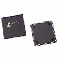
Z16C3516VSG Zilog, Z16C3516VSG Datasheet - Page 80

Z16C3516VSG
Manufacturer Part Number
Z16C3516VSG
Description
IC 16MHZ Z8500 CMOS ISCC 68-PLCC
Manufacturer
Zilog
Series
IUSC™r
Specifications of Z16C3516VSG
Controller Type
Serial Communications Controller (SCC)
Interface
USB
Voltage - Supply
4.75 V ~ 5.25 V
Current - Supply
50mA
Operating Temperature
0°C ~ 70°C
Mounting Type
Surface Mount
Package / Case
68-LCC (J-Lead)
Lead Free Status / RoHS Status
Lead free / RoHS Compliant
Other names
269-4690-5
Z16C3516VSG
Z16C3516VSG
Available stocks
Company
Part Number
Manufacturer
Quantity
Price
Company:
Part Number:
Z16C3516VSG
Manufacturer:
INTEL
Quantity:
6 219
- Current page: 80 of 268
- Download datasheet (3Mb)
Z16C35ISCC™ User’s Manual
Register Descriptions
5.5 READ REGISTERS (Continued)
Bit 7 is the Break/Abort Interrupt Enable
If this bit is set to “1,” a change in the Break/Abort status of
the receiver causes an External/Status interrupt. This bit is
set by a channel or hardware reset.
Bit 6 is the Transmit Underrun/EOM Interrupt Enable
If this bit is set to “1,” a change of state by the Tx Under-
run/EOM latch in the transmitter causes an External/Sta-
tus interrupt. This bit is set to “1” by a channel or hardware
reset.
5.5 READ REGISTERS
The ISCC SCC cell contains seven read registers in
each channel. In addition, there are two registers which
are shared by both channels. The status of these regis-
ters is continually changing and depends on the mode
of communication, received and transmitted data, and
the manner in which this data is transferred to and from
the CPU. The following description details the bit as-
signments for each register.
5.5.1 Read Register 0 (Transmit/receive
buffer Status and External Status)
Read Register 0 contains the status of the receive and
transmit buffers. RR0 also contains the status bits for the
six sources of External/Status interrupts. The bit configu-
ration is illustrated in Figure 5-18.
5-20
Write Register 15
D7
D6
D5 D4 D3 D2 D1 D0
Figure 5-17. Write Register 15
0
Zero Count IE
SDLC FIFO Enable
DCD IE
Sync/Hunt IE
CTS IE
Tx Underrun/EOM IE
Break/Abort IE
P R E L I M I N A R Y
Bit 5 is the CTS Interrupt Enable
If this bit is set to “1,” a change of state on the /CTS pin
causes an External/Status Interrupt. This bit is set by a
channel or hardware reset.
Bit 4 is the SYNC/Hunt Interrupt Enable
If this bit is set to “1,” a change of state on the /SYNC pin
causes an External/Status interrupt in Asynchronous
mode, and a change of state in the Hunt bit in the receiver
causes and External/Status interrupt in synchronous
modes. This bit is set by a channel or hardware reset.
Bit 3 is the DCD Interrupt Enable
If this bit is set to “1,” a change of state on the /DCD pin
causes an External/Status interrupt. This bit is set by a
channel or hardware reset.
Bit 2 is not used and must be programmed “0.”
Bit 1 is the Zero Count Interrupt Enable
If this bit is set to “1,” an External/Status interrupt is gener-
ated whenever the counter in the baud rate generator
reaches “0.” This bit is set to “0” by a channel or hardware
reset.
Bit 0 is not used and must be programmed “0.”
Read Register 0
D7
D6
D5 D4 D3 D2 D1 D0
Figure 5-18. Read Register 0
Rx Character Available
Zero Count
Tx Buffer Empty
DCD
Sync/Hunt
CTS
Tx Underrun/EOM
Break/Abort
UM011001-0601
Related parts for Z16C3516VSG
Image
Part Number
Description
Manufacturer
Datasheet
Request
R

Part Number:
Description:
CMOS ISCC INTEGRATED SERIAL COMMUNICATIONS CONTROLLER
Manufacturer:
ZILOG [Zilog, Inc.]
Datasheet:

Part Number:
Description:
Communication Controllers, ZILOG INTELLIGENT PERIPHERAL CONTROLLER (ZIP)
Manufacturer:
Zilog, Inc.
Datasheet:

Part Number:
Description:
KIT DEV FOR Z8 ENCORE 16K TO 64K
Manufacturer:
Zilog
Datasheet:

Part Number:
Description:
KIT DEV Z8 ENCORE XP 28-PIN
Manufacturer:
Zilog
Datasheet:

Part Number:
Description:
DEV KIT FOR Z8 ENCORE 8K/4K
Manufacturer:
Zilog
Datasheet:

Part Number:
Description:
KIT DEV Z8 ENCORE XP 28-PIN
Manufacturer:
Zilog
Datasheet:

Part Number:
Description:
DEV KIT FOR Z8 ENCORE 4K TO 8K
Manufacturer:
Zilog
Datasheet:

Part Number:
Description:
CMOS Z8 microcontroller. ROM 16 Kbytes, RAM 256 bytes, speed 16 MHz, 32 lines I/O, 3.0V to 5.5V
Manufacturer:
Zilog, Inc.
Datasheet:

Part Number:
Description:
Low-cost microcontroller. 512 bytes ROM, 61 bytes RAM, 8 MHz
Manufacturer:
Zilog, Inc.
Datasheet:

Part Number:
Description:
Z8 4K OTP Microcontroller
Manufacturer:
Zilog, Inc.
Datasheet:

Part Number:
Description:
CMOS SUPER8 ROMLESS MCU
Manufacturer:
Zilog, Inc.
Datasheet:

Part Number:
Description:
SL1866 CMOSZ8 OTP Microcontroller
Manufacturer:
Zilog, Inc.
Datasheet:

Part Number:
Description:
SL1866 CMOSZ8 OTP Microcontroller
Manufacturer:
Zilog, Inc.
Datasheet:

Part Number:
Description:
OTP (KB) = 1, RAM = 125, Speed = 12, I/O = 14, 8-bit Timers = 2, Comm Interfaces Other Features = Por, LV Protect, Voltage = 4.5-5.5V
Manufacturer:
Zilog, Inc.
Datasheet:


