MCP1631RD-DCPC1 Microchip Technology, MCP1631RD-DCPC1 Datasheet - Page 107
MCP1631RD-DCPC1
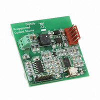
Manufacturer Part Number
MCP1631RD-DCPC1
Description
REF DES BATT CHARG OR LED DRIVER
Manufacturer
Microchip Technology
Datasheets
1.PIC16F616T-ISL.pdf
(214 pages)
2.MCP1631VHVT-330EST.pdf
(34 pages)
3.MCP1631VHVT-330EST.pdf
(32 pages)
Specifications of MCP1631RD-DCPC1
Current - Output / Channel
700mA
Outputs And Type
1, Non-Isolated
Features
Firmware for Li-Ion, NiMH, and NiCd Battery Charger
Voltage - Input
3.5 ~ 16 V
Utilized Ic / Part
MCP1631HV, PIC16F616
Core Chip
MCP1631HV, PIC16F616
Topology
Parallel, Series
Output Current
1A
No. Of Outputs
1
Input Voltage
3.5V To 16V
Dimming Control Type
Analog
Kit Contents
Board
Lead Free Status / RoHS Status
Lead free / RoHS Compliant
Voltage - Output
-
Lead Free Status / Rohs Status
Lead free / RoHS Compliant


11.0
The PIC16HV610/16HV616 include a permanent
internal 5 volt (nominal) shunt regulator in parallel with
the V
voltage
unregulated supply. All external devices connected
directly to the V
voltage and contribute to the total V
(I
11.1
A shunt regulator generates a specific supply voltage
by creating a voltage drop across a pass resistor R
The voltage at the V
monitored and compared to an internal voltage refer-
ence. The current through the resistor is then adjusted,
based on the result of the comparison, to produce a
voltage drop equal to the difference between the supply
voltage V
See Figure 11-1 for voltage regulator schematic.
FIGURE 11-1:
© 2009 Microchip Technology Inc.
LOAD
C
I
SUPPLY
BYPASS
DD
).
pin. This eliminates the need for an external
VOLTAGE REGULATOR
Regulator Operation
regulator
UNREG
V
UNREG
R
SER
I
DD
SHUNT
and the V
pin will share the regulated supply
in
DD
VOLTAGE REGULATOR
systems
pin of the microcontroller is
DD
of the microcontroller.
Feedback
sourced
DD
I
supply current
LOAD
PIC16F610/616/16HV610/616
by
V
V
DD
SS
SER
an
.
An external current limiting resistor, R
between the unregulated supply, V
pin, drops the difference in voltage between V
and V
defined by Equation 11-1.
EQUATION 11-1:
11.2
The supply voltage V
constant. Therefore, the current range of the regulator
is limited. Selecting a value for R
three factors into consideration.
Since the regulator uses the band gap voltage as the
regulated voltage reference, this voltage reference is
permanently enabled in the PIC16HV610/16HV616
devices.
Where:
R
R
VU
VU
V
I
1.05
0.95
LOAD
DD
MAX
MIN
MIN
MAX
DD
. R
Regulator Considerations
= maximum value of R
= minimum value of R
= minimum value of V
= maximum value of V
= regulated voltage (5V nominal)
= maximum expected load current in mA
= compensation for +5% tolerance of R
= compensation for -5% tolerance of R
R
R
SER
including I/O pin currents and external
circuits connected to V
MAX
MIN
must be between R
=
=
1.05 • (4
UNREG
0.95 • (50
R
(VU
(VU
SER
MAX
MIN
M
and load current are not
LIMITING RESISTOR
A + I
- 5V)
- 5V)
M
UNREG
SER
UNREG
SER
A)
SER
UNREG
LOAD
DD
DS41288F-page 107
(ohms)
MAX
(ohms)
.
must take these
)
, and the V
SER
and R
, located
UNREG
MIN
SER
SER
DD
as
Related parts for MCP1631RD-DCPC1
Image
Part Number
Description
Manufacturer
Datasheet
Request
R

Part Number:
Description:
REFERENCE DESIGN MCP1631HV
Manufacturer:
Microchip Technology
Datasheet:

Part Number:
Description:
REFERENCE DESIGN FOR MCP1631HV
Manufacturer:
Microchip Technology
Datasheet:

Part Number:
Description:
Manufacturer:
Microchip Technology Inc.
Datasheet:
Part Number:
Description:
Manufacturer:
Microchip Technology Inc.
Datasheet:
Part Number:
Description:
Manufacturer:
Microchip Technology Inc.
Datasheet:
Part Number:
Description:
Manufacturer:
Microchip Technology Inc.
Datasheet:
Part Number:
Description:
Manufacturer:
Microchip Technology Inc.
Datasheet:
Part Number:
Description:
Manufacturer:
Microchip Technology Inc.
Datasheet:
Part Number:
Description:
Manufacturer:
Microchip Technology Inc.
Datasheet:
Part Number:
Description:
Manufacturer:
Microchip Technology Inc.
Datasheet: