MCP1631RD-DCPC1 Microchip Technology, MCP1631RD-DCPC1 Datasheet - Page 75
MCP1631RD-DCPC1
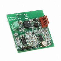
Manufacturer Part Number
MCP1631RD-DCPC1
Description
REF DES BATT CHARG OR LED DRIVER
Manufacturer
Microchip Technology
Datasheets
1.PIC16F616T-ISL.pdf
(214 pages)
2.MCP1631VHVT-330EST.pdf
(34 pages)
3.MCP1631VHVT-330EST.pdf
(32 pages)
Specifications of MCP1631RD-DCPC1
Current - Output / Channel
700mA
Outputs And Type
1, Non-Isolated
Features
Firmware for Li-Ion, NiMH, and NiCd Battery Charger
Voltage - Input
3.5 ~ 16 V
Utilized Ic / Part
MCP1631HV, PIC16F616
Core Chip
MCP1631HV, PIC16F616
Topology
Parallel, Series
Output Current
1A
No. Of Outputs
1
Input Voltage
3.5V To 16V
Dimming Control Type
Analog
Kit Contents
Board
Lead Free Status / RoHS Status
Lead free / RoHS Compliant
Voltage - Output
-
Lead Free Status / Rohs Status
Lead free / RoHS Compliant


FIGURE 9-2:
9.1.5
The ADC module allows for the ability to generate an
interrupt upon completion of an analog-to-digital
conversion. The ADC interrupt flag is the ADIF bit in the
PIR1 register. The ADC interrupt enable is the ADIE bit
in the PIE1 register. The ADIF bit must be cleared in
software.
This interrupt can be generated while the device is
operating or while in Sleep. If the device is in Sleep, the
interrupt will wake-up the device. Upon waking from
Sleep, the next instruction following the SLEEP
instruction is always executed. If the user is attempting
to wake-up from Sleep and resume in-line code
execution, the global interrupt must be disabled. If the
global interrupt is enabled, execution will switch to the
interrupt service routine.
Please see Section 9.1.5 “Interrupts” for more
information.
FIGURE 9-3:
© 2009 Microchip Technology Inc.
Note:
(ADFM = 0)
(ADFM = 1)
INTERRUPTS
The ADIF bit is set at the completion of
every conversion, regardless of whether
or not the ADC interrupt is enabled.
T
CY
Set GO/DONE bit
Holding Capacitor is Disconnected from Analog Input (typically 100 ns)
to T
AD
Conversion Starts
ANALOG-TO-DIGITAL CONVERSION T
10-BIT A/D CONVERSION RESULT FORMAT
MSB
bit 7
bit 7
T
AD
Unimplemented: Read as ‘0’
1 T
AD
b9
2 T
AD
b8
ADRESH
3 T
PIC16F610/616/16HV610/616
10-bit A/D Result
AD
b7
4 T
AD
b6
5 T
MSB
AD
b5
6 T
bit 0
bit 0
9.1.6
The 10-bit A/D conversion result can be supplied in two
formats, left justified or right justified. The ADFM bit of
the ADCON0 register controls the output format.
Figure 9-4 shows the two output formats.
ADRESH and ADRESL registers are loaded,
GO bit is cleared,
ADIF bit is set,
Holding capacitor is connected to analog input
AD
b4
7 T
AD
AD
b3
bit 7
bit 7
CYCLES
8 T
RESULT FORMATTING
10-bit A/D Result
LSB
AD
b2
9
T
AD
b1
Unimplemented: Read as ‘0’
10 T
ADRESL
AD
b0
11
DS41288F-page 75
bit 0
LSB
bit 0
Related parts for MCP1631RD-DCPC1
Image
Part Number
Description
Manufacturer
Datasheet
Request
R

Part Number:
Description:
REFERENCE DESIGN MCP1631HV
Manufacturer:
Microchip Technology
Datasheet:

Part Number:
Description:
REFERENCE DESIGN FOR MCP1631HV
Manufacturer:
Microchip Technology
Datasheet:

Part Number:
Description:
Manufacturer:
Microchip Technology Inc.
Datasheet:
Part Number:
Description:
Manufacturer:
Microchip Technology Inc.
Datasheet:
Part Number:
Description:
Manufacturer:
Microchip Technology Inc.
Datasheet:
Part Number:
Description:
Manufacturer:
Microchip Technology Inc.
Datasheet:
Part Number:
Description:
Manufacturer:
Microchip Technology Inc.
Datasheet:
Part Number:
Description:
Manufacturer:
Microchip Technology Inc.
Datasheet:
Part Number:
Description:
Manufacturer:
Microchip Technology Inc.
Datasheet:
Part Number:
Description:
Manufacturer:
Microchip Technology Inc.
Datasheet: