MCP1631RD-DCPC1 Microchip Technology, MCP1631RD-DCPC1 Datasheet - Page 39
MCP1631RD-DCPC1
Manufacturer Part Number
MCP1631RD-DCPC1
Description
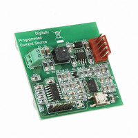
REF DES BATT CHARG OR LED DRIVER
Manufacturer
Microchip Technology
Datasheets
1.PIC16F616T-ISL.pdf
(214 pages)
2.MCP1631VHVT-330EST.pdf
(34 pages)
3.MCP1631VHVT-330EST.pdf
(32 pages)
Specifications of MCP1631RD-DCPC1
Current - Output / Channel
700mA
Outputs And Type
1, Non-Isolated
Features
Firmware for Li-Ion, NiMH, and NiCd Battery Charger
Voltage - Input
3.5 ~ 16 V
Utilized Ic / Part
MCP1631HV, PIC16F616
Core Chip
MCP1631HV, PIC16F616
Topology
Parallel, Series
Output Current
1A
No. Of Outputs
1
Input Voltage
3.5V To 16V
Dimming Control Type
Analog
Kit Contents
Board
Lead Free Status / RoHS Status
Lead free / RoHS Compliant
Voltage - Output
-
Lead Free Status / Rohs Status
Lead free / RoHS Compliant


4.2.4.5
Figure 4-4 shows the diagram for this pin. The RA4 pin
is configurable to function as one of the following:
• a general purpose I/O
• an analog input for the ADC
FIGURE 4-4:
© 2009 Microchip Technology Inc.
Interrupt-on-
RA4/AN3
Note 1: CLK modes are XT, HS, LP, TMR1 LP and CLKOUT Enable.
Change
2: With CLKOUT option.
3: Analog Input mode comes from ANSEL.
4: Set has priority over Reset.
5: PIC16F616/16HV616 only.
BLOCK DIAGRAM OF RA4
Write ‘0’ to RAIF
(1)
/T1G/OSC2/CLKOUT
(1)
Q
S
R
(4)
Data Bus
PORTA
PORTA
WPUA
WPUA
TRISA
TRISA
IOCA
IOCA
PIC16F610/616/16HV610/616
WR
WR
WR
WR
RD
RD
RD
RD
RA<5, 3:0> pins
From other
D
D
D
D
CK
CK
CK
CK
Q
Q
Q
Q
Q
Q
Q
Q
To T1G
To A/D Converter
• a Timer1 gate (count enable)
• a crystal/resonator connection
• a clock output
Note 1: PIC16F616/16HV616 only.
Input Mode
Analog
OSC1
F
(5)
OSC
INTOSC/
RC/EC
CLKOUT
CLKOUT
Enable
(3)
Enable
Input Mode
/4
RD PORTA
RAPU
CLKOUT
Analog
Enable
Oscillator
Circuit
Modes
Q
Q
1
0
(2)
CLK
EN
EN
(1)
D
D
V
DD
Weak
V
V
Q1
DD
SS
I/O Pin
DS41288F-page 39
Related parts for MCP1631RD-DCPC1
Image
Part Number
Description
Manufacturer
Datasheet
Request
R

Part Number:
Description:
REFERENCE DESIGN MCP1631HV
Manufacturer:
Microchip Technology
Datasheet:

Part Number:
Description:
REFERENCE DESIGN FOR MCP1631HV
Manufacturer:
Microchip Technology
Datasheet:

Part Number:
Description:
Manufacturer:
Microchip Technology Inc.
Datasheet:
Part Number:
Description:
Manufacturer:
Microchip Technology Inc.
Datasheet:
Part Number:
Description:
Manufacturer:
Microchip Technology Inc.
Datasheet:
Part Number:
Description:
Manufacturer:
Microchip Technology Inc.
Datasheet:
Part Number:
Description:
Manufacturer:
Microchip Technology Inc.
Datasheet:
Part Number:
Description:
Manufacturer:
Microchip Technology Inc.
Datasheet:
Part Number:
Description:
Manufacturer:
Microchip Technology Inc.
Datasheet:
Part Number:
Description:
Manufacturer:
Microchip Technology Inc.
Datasheet: