MCP1631RD-DCPC1 Microchip Technology, MCP1631RD-DCPC1 Datasheet - Page 78
MCP1631RD-DCPC1
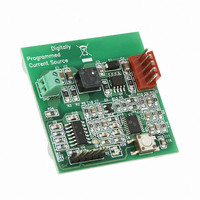
Manufacturer Part Number
MCP1631RD-DCPC1
Description
REF DES BATT CHARG OR LED DRIVER
Manufacturer
Microchip Technology
Datasheets
1.PIC16F616T-ISL.pdf
(214 pages)
2.MCP1631VHVT-330EST.pdf
(34 pages)
3.MCP1631VHVT-330EST.pdf
(32 pages)
Specifications of MCP1631RD-DCPC1
Current - Output / Channel
700mA
Outputs And Type
1, Non-Isolated
Features
Firmware for Li-Ion, NiMH, and NiCd Battery Charger
Voltage - Input
3.5 ~ 16 V
Utilized Ic / Part
MCP1631HV, PIC16F616
Core Chip
MCP1631HV, PIC16F616
Topology
Parallel, Series
Output Current
1A
No. Of Outputs
1
Input Voltage
3.5V To 16V
Dimming Control Type
Analog
Kit Contents
Board
Lead Free Status / RoHS Status
Lead free / RoHS Compliant
Voltage - Output
-
Lead Free Status / Rohs Status
Lead free / RoHS Compliant


PIC16F610/616/16HV610/616
9.2.7
The following registers are used to control the operation of the ADC.
REGISTER 9-1:
DS41288F-page 78
bit 7
Legend:
R = Readable bit
-n = Value at POR
bit 7
bit 6
bit 5-2
bit 1
bit 0
Note 1:
ADFM
R/W-0
When the CHS<3:0> bits change to select the 1.2V or 0.6V Fixed Voltage Reference, the reference output voltage will
have a transient. If the Comparator module uses this VP6 reference voltage, the comparator output may momentarily
change state due to the transient.
ADC REGISTER DEFINITIONS
ADFM: A/D Conversion Result Format Select bit
1 = Right justified
0 = Left justified
VCFG: Voltage Reference bit
1 = V
0 = V
CHS<3:0>: Analog Channel Select bits
0000 = Channel 00 (AN0)
0001 = Channel 01 (AN1)
0010 = Channel 02 (AN2)
0011 = Channel 03 (AN3)
0100 = Channel 04 (AN4)
0101 = Channel 05 (AN5)
0110 = Channel 06 (AN6)
0111 = Channel 07 (AN7)
1000 = Reserved – do not use
1001 = Reserved – do not use
1010 = Reserved – do not use
1011 = Reserved – do not use
1100 = CV
1101 = 0.6V Fixed Voltage Reference
1110 = 1.2V Fixed Voltage Reference
1111 = Reserved – do not use
GO/DONE: A/D Conversion Status bit
1 = A/D conversion cycle in progress. Setting this bit starts an A/D conversion cycle.
0 = A/D conversion completed/not in progress
ADON: ADC Enable bit
1 = ADC is enabled
0 = ADC is disabled and consumes no operating current
VCFG
This bit is automatically cleared by hardware when the A/D conversion has completed.
R/W-0
REF
DD
ADCON0: A/D CONTROL REGISTER 0
pin
REF
W = Writable bit
‘1’ = Bit is set
CHS3
R/W-0
CHS2
R/W-0
(1)
(1)
U = Unimplemented bit, read as ‘0’
‘0’ = Bit is cleared
CHS1
R/W-0
CHS0
R/W-0
© 2009 Microchip Technology Inc.
x = Bit is unknown
GO/DONE
R/W-0
ADON
R/W-0
bit 0
Related parts for MCP1631RD-DCPC1
Image
Part Number
Description
Manufacturer
Datasheet
Request
R

Part Number:
Description:
REFERENCE DESIGN MCP1631HV
Manufacturer:
Microchip Technology
Datasheet:

Part Number:
Description:
REFERENCE DESIGN FOR MCP1631HV
Manufacturer:
Microchip Technology
Datasheet:

Part Number:
Description:
Manufacturer:
Microchip Technology Inc.
Datasheet:
Part Number:
Description:
Manufacturer:
Microchip Technology Inc.
Datasheet:
Part Number:
Description:
Manufacturer:
Microchip Technology Inc.
Datasheet:
Part Number:
Description:
Manufacturer:
Microchip Technology Inc.
Datasheet:
Part Number:
Description:
Manufacturer:
Microchip Technology Inc.
Datasheet:
Part Number:
Description:
Manufacturer:
Microchip Technology Inc.
Datasheet:
Part Number:
Description:
Manufacturer:
Microchip Technology Inc.
Datasheet:
Part Number:
Description:
Manufacturer:
Microchip Technology Inc.
Datasheet: