MCP1631RD-DCPC1 Microchip Technology, MCP1631RD-DCPC1 Datasheet - Page 158
MCP1631RD-DCPC1
Manufacturer Part Number
MCP1631RD-DCPC1
Description
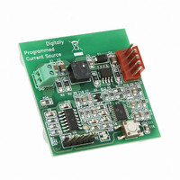
REF DES BATT CHARG OR LED DRIVER
Manufacturer
Microchip Technology
Datasheets
1.PIC16F616T-ISL.pdf
(214 pages)
2.MCP1631VHVT-330EST.pdf
(34 pages)
3.MCP1631VHVT-330EST.pdf
(32 pages)
Specifications of MCP1631RD-DCPC1
Current - Output / Channel
700mA
Outputs And Type
1, Non-Isolated
Features
Firmware for Li-Ion, NiMH, and NiCd Battery Charger
Voltage - Input
3.5 ~ 16 V
Utilized Ic / Part
MCP1631HV, PIC16F616
Core Chip
MCP1631HV, PIC16F616
Topology
Parallel, Series
Output Current
1A
No. Of Outputs
1
Input Voltage
3.5V To 16V
Dimming Control Type
Analog
Kit Contents
Board
Lead Free Status / RoHS Status
Lead free / RoHS Compliant
Voltage - Output
-
Lead Free Status / Rohs Status
Lead free / RoHS Compliant


PIC16F610/616/16HV610/616
TABLE 15-2:
DS41288F-page 158
Standard Operating Conditions (unless otherwise stated)
Operating Temperature
OS06
OS07
OS08
OS10*
Note 1:
Param
No.
2:
3:
*
†
T
INT
INT
T
These parameters are characterized but not tested.
Data in “Typ” column is at 5.0V, 25°C unless otherwise stated. These parameters are for design guidance only and are
not tested.
Instruction cycle period (T
characterization data for that particular oscillator type under standard operating conditions with the device executing
code. Exceeding these specified limits may result in an unstable oscillator operation and/or higher than expected
current consumption. All devices are tested to operate at “min” values with an external clock applied to the OSC1 pin.
When an external clock input is used, the “max” cycle time limit is “DC” (no clock) for all devices.
To ensure these oscillator frequency tolerances, V
possible. 0.1 μF and 0.01 μF values in parallel are recommended.
By design.
WARM
IOSC ST
Sym
OSC
OSC
OSCILLATOR PARAMETERS
Internal Oscillator Switch
when running
Internal Calibrated
INTOSC Frequency
(4MHz)
Internal Calibrated
INTOSC Frequency
(8MHz)
INTOSC Oscillator Wake-
up from Sleep
Start-up Time
Characteristic
-40°C ≤ T
(3)
CY
A
) equals four times the input oscillator time base period. All specified values are based on
≤ +125°C
(2)
(2)
Tolerance
Freq.
±1%
±2%
±5%
±1%
±2%
±5%
—
—
—
—
DD
and V
3.96
3.92
3.80
7.92
7.84
7.60
Min
5.5
3.5
—
3
SS
must be capacitively decoupled as close to the device as
Typ†
4.0
4.0
4.0
8.0
8.0
8.0
12
—
7
6
Max
4.04
4.08
8.08
8.16
8.40
4.2
24
14
11
2
Units
T
MHz
MHz
MHz
MHz
MHz
MHz
OSC
μs
μs
μs
© 2009 Microchip Technology Inc.
Slowest clock
V
2.5V ≤ V
0°C ≤ T
2.0V ≤ V
-40°C ≤ T
-40°C ≤ T
V
2.5V ≤ V
0°C ≤ T
2.0V ≤ V
-40°C ≤ T
-40°C ≤ T
V
V
V
DD
DD
DD
DD
DD
= 3.5V, T
= 3.5V, T
= 2.0V, -40°C to +85°C
= 3.0V, -40°C to +85°C
= 5.0V, -40°C to +85°C
A
A
DD
DD
DD
DD
Conditions
≤ +85°C
≤ +85°C
A
A
A
A
≤ +85°C (Ind.),
≤ +125°C (Ext.)
≤ +85°C (Ind.),
≤ +125°C (Ext.)
≤ 5.5V,
≤ 5.5V,
≤ 5.5V,
≤ 5.5V,
A
A
= 25°C
= 25°C
Related parts for MCP1631RD-DCPC1
Image
Part Number
Description
Manufacturer
Datasheet
Request
R

Part Number:
Description:
REFERENCE DESIGN MCP1631HV
Manufacturer:
Microchip Technology
Datasheet:

Part Number:
Description:
REFERENCE DESIGN FOR MCP1631HV
Manufacturer:
Microchip Technology
Datasheet:

Part Number:
Description:
Manufacturer:
Microchip Technology Inc.
Datasheet:
Part Number:
Description:
Manufacturer:
Microchip Technology Inc.
Datasheet:
Part Number:
Description:
Manufacturer:
Microchip Technology Inc.
Datasheet:
Part Number:
Description:
Manufacturer:
Microchip Technology Inc.
Datasheet:
Part Number:
Description:
Manufacturer:
Microchip Technology Inc.
Datasheet:
Part Number:
Description:
Manufacturer:
Microchip Technology Inc.
Datasheet:
Part Number:
Description:
Manufacturer:
Microchip Technology Inc.
Datasheet:
Part Number:
Description:
Manufacturer:
Microchip Technology Inc.
Datasheet: