MCP1631RD-DCPC1 Microchip Technology, MCP1631RD-DCPC1 Datasheet - Page 65
MCP1631RD-DCPC1
Manufacturer Part Number
MCP1631RD-DCPC1
Description
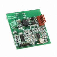
REF DES BATT CHARG OR LED DRIVER
Manufacturer
Microchip Technology
Datasheets
1.PIC16F616T-ISL.pdf
(214 pages)
2.MCP1631VHVT-330EST.pdf
(34 pages)
3.MCP1631VHVT-330EST.pdf
(32 pages)
Specifications of MCP1631RD-DCPC1
Current - Output / Channel
700mA
Outputs And Type
1, Non-Isolated
Features
Firmware for Li-Ion, NiMH, and NiCd Battery Charger
Voltage - Input
3.5 ~ 16 V
Utilized Ic / Part
MCP1631HV, PIC16F616
Core Chip
MCP1631HV, PIC16F616
Topology
Parallel, Series
Output Current
1A
No. Of Outputs
1
Input Voltage
3.5V To 16V
Dimming Control Type
Analog
Kit Contents
Board
Lead Free Status / RoHS Status
Lead free / RoHS Compliant
Voltage - Output
-
Lead Free Status / Rohs Status
Lead free / RoHS Compliant


8.8
There are three additional comparator features:
• Timer1 count enable (gate)
• Synchronizing output with Timer1
• Simultaneous read of comparator outputs
8.8.1
This feature can be used to time the duration or interval
of analog events. Clearing the T1GSS bit of the
CM2CON1 register will enable Timer1 to increment
based on the output of Comparator C2. This requires
that Timer1 is on and gating is enabled. See
Section 6.0 “Timer1 Module with Gate Control” for
details.
It is recommended to synchronize the comparator with
Timer1 by setting the C2SYNC bit when the comparator
is used as the Timer1 gate source. This ensures Timer1
does not miss an increment if the comparator changes
during an increment.
REGISTER 8-3:
© 2009 Microchip Technology Inc.
bit 7
Legend:
R = Readable bit
-n = Value at POR
bit 7
bit 6
bit 5
bit 4
bit 3
bit 2
bit 1
bit 0
MC1OUT
R-0
Additional Comparator Features
COMPARATOR C2 GATING TIMER1
MC1OUT: Mirror Copy of C1OUT bit
MC2OUT: Mirror Copy of C2OUT bit
Unimplemented: Read as ‘0’
T1ACS: Timer1 Alternate Clock Select bit
1 = Timer1 clock source is the system clock (F
0 = Timer1 clock source is the internal clock F
C1HYS: Comparator C1 Hysteresis Enable bit
1 = Comparator C1 Hysteresis enabled
0 = Comparator C1 Hysteresis disabled
C2HYS: Comparator C2 Hysteresis Enable bit
1 = Comparator C2 Hysteresis enabled
0 = Comparator C2 Hysteresis disabled
T1GSS: Timer1 Gate Source Select bit
1 = Timer1 gate source is T1G
0 = Timer1 gate source is SYNCC2OUT.
C2SYNC: Comparator C2 Output Synchronization bit
1 = C2 Output is synchronous to falling edge of Timer1 clock
0 = C2 Output is asynchronous
MC2OUT
R-0
CM2CON1: COMPARATOR 2 CONTROL REGISTER 1
W = Writable bit
‘1’ = Bit is set
U-0
—
PIC16F610/616/16HV610/616
T1ACS
R/W-0
OSC
OSC
U = Unimplemented bit, read as ‘0’
‘0’ = Bit is cleared
/4)
)
C1HYS
8.8.2
The Comparator C2 output can be synchronized with
Timer1 by setting the C2SYNC bit of the CM2CON1
register. When enabled, the C2 output is latched on the
falling edge of the Timer1 clock source. If a prescaler is
used with Timer1, the comparator output is latched after
the prescaling function. To prevent a race condition, the
comparator output is latched on the falling edge of the
Timer1 clock source and Timer1 increments on the
rising edge of its clock source. See the Comparator
Block Diagram (Figure 8-3) and the Timer1 Block
Diagram (Figure 6-1) for more information.
8.8.3
The MC1OUT and MC2OUT bits of the CM2CON1
register are mirror copies of both comparator outputs.
The ability to read both outputs simultaneously from a
single register eliminates the timing skew of reading
separate registers.
R/W-0
Note 1: Obtaining the status of C1OUT or C2OUT
SYNCHRONIZING COMPARATOR
C2 OUTPUT TO TIMER1
SIMULTANEOUS COMPARATOR
OUTPUT READ
by reading CM2CON1 does not affect the
comparator interrupt mismatch registers.
C2HYS
R/W-0
x = Bit is unknown
T1GSS
R/W-1
DS41288F-page 65
C2SYNC
R/W-0
bit 0
Related parts for MCP1631RD-DCPC1
Image
Part Number
Description
Manufacturer
Datasheet
Request
R

Part Number:
Description:
REFERENCE DESIGN MCP1631HV
Manufacturer:
Microchip Technology
Datasheet:

Part Number:
Description:
REFERENCE DESIGN FOR MCP1631HV
Manufacturer:
Microchip Technology
Datasheet:

Part Number:
Description:
Manufacturer:
Microchip Technology Inc.
Datasheet:
Part Number:
Description:
Manufacturer:
Microchip Technology Inc.
Datasheet:
Part Number:
Description:
Manufacturer:
Microchip Technology Inc.
Datasheet:
Part Number:
Description:
Manufacturer:
Microchip Technology Inc.
Datasheet:
Part Number:
Description:
Manufacturer:
Microchip Technology Inc.
Datasheet:
Part Number:
Description:
Manufacturer:
Microchip Technology Inc.
Datasheet:
Part Number:
Description:
Manufacturer:
Microchip Technology Inc.
Datasheet:
Part Number:
Description:
Manufacturer:
Microchip Technology Inc.
Datasheet: