MCP1631RD-DCPC1 Microchip Technology, MCP1631RD-DCPC1 Datasheet - Page 47
MCP1631RD-DCPC1
Manufacturer Part Number
MCP1631RD-DCPC1
Description
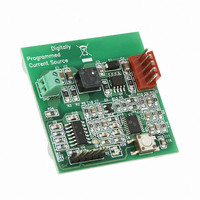
REF DES BATT CHARG OR LED DRIVER
Manufacturer
Microchip Technology
Datasheets
1.PIC16F616T-ISL.pdf
(214 pages)
2.MCP1631VHVT-330EST.pdf
(34 pages)
3.MCP1631VHVT-330EST.pdf
(32 pages)
Specifications of MCP1631RD-DCPC1
Current - Output / Channel
700mA
Outputs And Type
1, Non-Isolated
Features
Firmware for Li-Ion, NiMH, and NiCd Battery Charger
Voltage - Input
3.5 ~ 16 V
Utilized Ic / Part
MCP1631HV, PIC16F616
Core Chip
MCP1631HV, PIC16F616
Topology
Parallel, Series
Output Current
1A
No. Of Outputs
1
Input Voltage
3.5V To 16V
Dimming Control Type
Analog
Kit Contents
Board
Lead Free Status / RoHS Status
Lead free / RoHS Compliant
Voltage - Output
-
Lead Free Status / Rohs Status
Lead free / RoHS Compliant


REGISTER 5-1:
TABLE 5-1:
© 2009 Microchip Technology Inc.
TMR0
INTCON
OPTION_REG
TRISA
Legend: – = Unimplemented locations, read as ‘0’, u = unchanged, x = unknown. Shaded cells are not used by the
bit 7
Legend:
R = Readable bit
-n = Value at POR
bit 7
bit 6
bit 5
bit 4
bit 3
bit 2-0
R/W-1
RAPU
Name
Timer0 module.
RAPU: PORTA Pull-up Enable bit
1 = PORTA pull-ups are disabled
0 = PORTA pull-ups are enabled by individual PORT latch values
INTEDG: Interrupt Edge Select bit
1 = Interrupt on rising edge of INT pin
0 = Interrupt on falling edge of INT pin
T0CS: TMR0 Clock Source Select bit
1 = Transition on T0CKI pin
0 = Internal instruction cycle clock (F
T0SE: TMR0 Source Edge Select bit
1 = Increment on high-to-low transition on T0CKI pin
0 = Increment on low-to-high transition on T0CKI pin
PSA: Prescaler Assignment bit
1 = Prescaler is assigned to the WDT
0 = Prescaler is assigned to the Timer0 module
PS<2:0>: Prescaler Rate Select bits
Timer0 Modules Register
RAPU INTEDG
SUMMARY OF REGISTERS ASSOCIATED WITH TIMER0
Bit 7
INTEDG
GIE
R/W-1
—
OPTION_REG: OPTION REGISTER
BIT VALUE
PEIE
Bit 6
000
001
010
011
100
101
110
111
—
W = Writable bit
‘1’ = Bit is set
R/W-1
T0CS
TRISA5 TRISA4 TRISA3 TRISA2 TRISA1 TRISA0 --11 1111 --11 1111
T0CS
Bit 5
TMR0 RATE
T0IE
1 : 2
1 : 4
1 : 8
1 : 16
1 : 32
1 : 64
1 : 128
1 : 256
PIC16F610/616/16HV610/616
T0SE
Bit 4
INTE
R/W-1
T0SE
WDT RATE
1 : 1
1 : 2
1 : 4
1 : 8
1 : 16
1 : 32
1 : 64
1 : 128
OSC
RAIE
Bit 3
PSA
/4)
U = Unimplemented bit, read as ‘0’
‘0’ = Bit is cleared
R/W-1
PSA
Bit 2
T0IF
PS2
INTF
Bit 1
PS1
R/W-1
PS2
RAIF
Bit 0
PS0
x = Bit is unknown
xxxx xxxx uuuu uuuu
0000 0000 0000 0000
1111 1111 1111 1111
POR, BOR
Value on
R/W-1
PS1
DS41288F-page 47
Value on
all other
Resets
R/W-1
PS0
bit 0
Related parts for MCP1631RD-DCPC1
Image
Part Number
Description
Manufacturer
Datasheet
Request
R

Part Number:
Description:
REFERENCE DESIGN MCP1631HV
Manufacturer:
Microchip Technology
Datasheet:

Part Number:
Description:
REFERENCE DESIGN FOR MCP1631HV
Manufacturer:
Microchip Technology
Datasheet:

Part Number:
Description:
Manufacturer:
Microchip Technology Inc.
Datasheet:
Part Number:
Description:
Manufacturer:
Microchip Technology Inc.
Datasheet:
Part Number:
Description:
Manufacturer:
Microchip Technology Inc.
Datasheet:
Part Number:
Description:
Manufacturer:
Microchip Technology Inc.
Datasheet:
Part Number:
Description:
Manufacturer:
Microchip Technology Inc.
Datasheet:
Part Number:
Description:
Manufacturer:
Microchip Technology Inc.
Datasheet:
Part Number:
Description:
Manufacturer:
Microchip Technology Inc.
Datasheet:
Part Number:
Description:
Manufacturer:
Microchip Technology Inc.
Datasheet: