MCP1631RD-DCPC1 Microchip Technology, MCP1631RD-DCPC1 Datasheet - Page 90
MCP1631RD-DCPC1
Manufacturer Part Number
MCP1631RD-DCPC1
Description
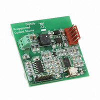
REF DES BATT CHARG OR LED DRIVER
Manufacturer
Microchip Technology
Datasheets
1.PIC16F616T-ISL.pdf
(214 pages)
2.MCP1631VHVT-330EST.pdf
(34 pages)
3.MCP1631VHVT-330EST.pdf
(32 pages)
Specifications of MCP1631RD-DCPC1
Current - Output / Channel
700mA
Outputs And Type
1, Non-Isolated
Features
Firmware for Li-Ion, NiMH, and NiCd Battery Charger
Voltage - Input
3.5 ~ 16 V
Utilized Ic / Part
MCP1631HV, PIC16F616
Core Chip
MCP1631HV, PIC16F616
Topology
Parallel, Series
Output Current
1A
No. Of Outputs
1
Input Voltage
3.5V To 16V
Dimming Control Type
Analog
Kit Contents
Board
Lead Free Status / RoHS Status
Lead free / RoHS Compliant
Voltage - Output
-
Lead Free Status / Rohs Status
Lead free / RoHS Compliant


PIC16F610/616/16HV610/616
10.3
The PWM mode generates a Pulse-Width Modulated
signal on the CCP1 pin. The duty cycle, period and
resolution are determined by the following registers:
• PR2
• T2CON
• CCPR1L
• CCP1CON
In Pulse-Width Modulation (PWM) mode, the CCP
module produces up to a 10-bit resolution PWM output
on the CCP1 pin. Since the CCP1 pin is multiplexed
with the PORT data latch, the TRIS for that pin must be
cleared to make the CCP1 pin an output.
Figure 10-3 shows a simplified block diagram of PWM
operation.
Figure 10-4 shows a typical waveform of the PWM
signal.
For a step-by-step procedure on how to set up the CCP
module for PWM operation, see Section 10.3.7
“Setup for PWM Operation”.
FIGURE 10-3:
DS41288F-page 90
Note 1:
Note:
CCPR1H
Duty Cycle Registers
Comparator
2:
CCPR1L
PWM Mode
PR2
TMR2
Comparator
Clearing the CCP1CON register will
relinquish CCP1 control of the CCP1 pin.
The 8-bit timer TMR2 register is concatenated
with the 2-bit internal system clock (F
2 bits of the prescaler, to create the 10-bit time
base.
In PWM mode, CCPR1H is a read-only register.
(2)
(Slave)
(1)
SIMPLIFIED PWM BLOCK
DIAGRAM
Clear Timer2,
toggle CCP1 pin and
latch duty cycle
CCP1CON<5:4>
S
R
Q
TRIS
OSC
CCP1
), or
The PWM output (Figure 10-4) has a time base
(period) and a time that the output stays high (duty
cycle).
FIGURE 10-4:
Pulse Width
TMR2 = 0
Period
CCP PWM OUTPUT
TMR2 = CCPR1L:CCP1CON<5:4>
© 2009 Microchip Technology Inc.
TMR2 = PR2
Related parts for MCP1631RD-DCPC1
Image
Part Number
Description
Manufacturer
Datasheet
Request
R

Part Number:
Description:
REFERENCE DESIGN MCP1631HV
Manufacturer:
Microchip Technology
Datasheet:

Part Number:
Description:
REFERENCE DESIGN FOR MCP1631HV
Manufacturer:
Microchip Technology
Datasheet:

Part Number:
Description:
Manufacturer:
Microchip Technology Inc.
Datasheet:
Part Number:
Description:
Manufacturer:
Microchip Technology Inc.
Datasheet:
Part Number:
Description:
Manufacturer:
Microchip Technology Inc.
Datasheet:
Part Number:
Description:
Manufacturer:
Microchip Technology Inc.
Datasheet:
Part Number:
Description:
Manufacturer:
Microchip Technology Inc.
Datasheet:
Part Number:
Description:
Manufacturer:
Microchip Technology Inc.
Datasheet:
Part Number:
Description:
Manufacturer:
Microchip Technology Inc.
Datasheet:
Part Number:
Description:
Manufacturer:
Microchip Technology Inc.
Datasheet: