MCP1631RD-DCPC1 Microchip Technology, MCP1631RD-DCPC1 Datasheet - Page 118
MCP1631RD-DCPC1
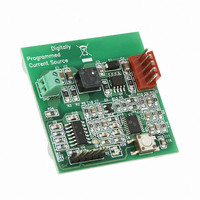
Manufacturer Part Number
MCP1631RD-DCPC1
Description
REF DES BATT CHARG OR LED DRIVER
Manufacturer
Microchip Technology
Datasheets
1.PIC16F616T-ISL.pdf
(214 pages)
2.MCP1631VHVT-330EST.pdf
(34 pages)
3.MCP1631VHVT-330EST.pdf
(32 pages)
Specifications of MCP1631RD-DCPC1
Current - Output / Channel
700mA
Outputs And Type
1, Non-Isolated
Features
Firmware for Li-Ion, NiMH, and NiCd Battery Charger
Voltage - Input
3.5 ~ 16 V
Utilized Ic / Part
MCP1631HV, PIC16F616
Core Chip
MCP1631HV, PIC16F616
Topology
Parallel, Series
Output Current
1A
No. Of Outputs
1
Input Voltage
3.5V To 16V
Dimming Control Type
Analog
Kit Contents
Board
Lead Free Status / RoHS Status
Lead free / RoHS Compliant
Voltage - Output
-
Lead Free Status / Rohs Status
Lead free / RoHS Compliant


PIC16F610/616/16HV610/616
12.4
The
sources of interrupt:
• External Interrupt RA2/INT
• Timer0 Overflow Interrupt
• PORTA Change Interrupts
• 2 Comparator Interrupts
• A/D Interrupt (PIC16F616/16HV616 only)
• Timer1 Overflow Interrupt
• Timer2 Match Interrupt (PIC16F616/16HV616 only)
• Enhanced CCP Interrupt (PIC16F616/16HV616
The Interrupt Control register (INTCON) and Peripheral
Interrupt Request Register 1 (PIR1) record individual
interrupt requests in flag bits. The INTCON register
also has individual and global interrupt enable bits.
The Global Interrupt Enable bit, GIE of the INTCON
register, enables (if set) all unmasked interrupts, or
disables (if cleared) all interrupts. Individual interrupts
can be disabled through their corresponding enable
bits in the INTCON register and PIE1 register. GIE is
cleared on Reset.
When an interrupt is serviced, the following actions
occur automatically:
• The GIE is cleared to disable any further interrupt.
• The return address is pushed onto the stack.
• The PC is loaded with 0004h.
The Return from Interrupt instruction, RETFIE, exits
the interrupt routine, as well as sets the GIE bit, which
re-enables unmasked interrupts.
The following interrupt flags are contained in the INT-
CON register:
• INT Pin Interrupt
• PORTA Change Interrupt
• Timer0 Overflow Interrupt
The peripheral interrupt flags are contained in the
special register, PIR1. The corresponding interrupt
enable bit is contained in special register, PIE1.
The following interrupt flags are contained in the PIR1
register:
• A/D Interrupt
• 2 Comparator Interrupts
• Timer1 Overflow Interrupt
• Timer2 Match Interrupt
• Enhanced CCP Interrupt
DS41288F-page 118
only)
PIC16F610/616/16HV610/616
Interrupts
has
multiple
For external interrupt events, such as the INT pin or
PORTA change interrupt, the interrupt latency will be
three or four instruction cycles. The exact latency
depends upon when the interrupt event occurs (see
Figure 12-8). The latency is the same for one or two-
cycle instructions. Once in the Interrupt Service
Routine, the source(s) of the interrupt can be
determined by polling the interrupt flag bits. The
interrupt flag bit(s) must be cleared in software before
re-enabling interrupts to avoid multiple interrupt
requests.
For
comparators, ADC, Enhanced CCP modules, refer to
the respective peripheral section.
12.4.1
The external interrupt on the RA2/INT pin is edge-
triggered; either on the rising edge if the INTEDG bit of
the OPTION register is set, or the falling edge, if the
INTEDG bit is clear. When a valid edge appears on the
RA2/INT pin, the INTF bit of the INTCON register is set.
This interrupt can be disabled by clearing the INTE
control bit of the INTCON register. The INTF bit must
be cleared by software in the Interrupt Service Routine
before re-enabling this interrupt. The RA2/INT interrupt
can wake-up the processor from Sleep, if the INTE bit
was set prior to going into Sleep. See Section 12.7
“Power-Down Mode (Sleep)” for details on Sleep and
Figure 12-9 for timing of wake-up from Sleep through
RA2/INT interrupt.
Note:
Note 1: Individual interrupt flag bits are set,
additional
2: When an instruction that clears the GIE
RA2/INT INTERRUPT
The ANSEL register must be initialized to
configure an analog channel as a digital
input. Pins configured as analog inputs will
read ‘0’ and cannot generate an interrupt.
regardless
corresponding mask bit or the GIE bit.
bit is executed, any interrupts that were
pending for execution in the next cycle
are ignored. The interrupts, which were
ignored, are still pending to be serviced
when the GIE bit is set again.
information
© 2009 Microchip Technology Inc.
of
the
on
status
Timer1,
of
Timer2,
their
Related parts for MCP1631RD-DCPC1
Image
Part Number
Description
Manufacturer
Datasheet
Request
R

Part Number:
Description:
REFERENCE DESIGN MCP1631HV
Manufacturer:
Microchip Technology
Datasheet:

Part Number:
Description:
REFERENCE DESIGN FOR MCP1631HV
Manufacturer:
Microchip Technology
Datasheet:

Part Number:
Description:
Manufacturer:
Microchip Technology Inc.
Datasheet:
Part Number:
Description:
Manufacturer:
Microchip Technology Inc.
Datasheet:
Part Number:
Description:
Manufacturer:
Microchip Technology Inc.
Datasheet:
Part Number:
Description:
Manufacturer:
Microchip Technology Inc.
Datasheet:
Part Number:
Description:
Manufacturer:
Microchip Technology Inc.
Datasheet:
Part Number:
Description:
Manufacturer:
Microchip Technology Inc.
Datasheet:
Part Number:
Description:
Manufacturer:
Microchip Technology Inc.
Datasheet:
Part Number:
Description:
Manufacturer:
Microchip Technology Inc.
Datasheet: