MC56F8037EVM Freescale Semiconductor, MC56F8037EVM Datasheet - Page 103
MC56F8037EVM
Manufacturer Part Number
MC56F8037EVM
Description
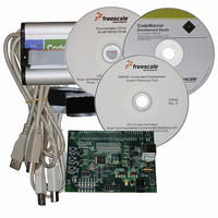
BOARD EVAL FOR MC56F8037
Manufacturer
Freescale Semiconductor
Type
MCUr
Datasheet
1.MC56F8037EVM.pdf
(180 pages)
Specifications of MC56F8037EVM
Contents
Board, Cables, CD, Debugger
Silicon Manufacturer
Freescale
Core Architecture
56800/E
Core Sub-architecture
56800/E
Silicon Core Number
MC56F
Silicon Family Name
MC56F80xx
Kit Contents
MC56F8037EVM, USB-JTAG Adapter, Cables, CD
Rohs Compliant
Yes
For Use With/related Products
MC56F8037
Lead Free Status / RoHS Status
Lead free / RoHS Compliant
Available stocks
Company
Part Number
Manufacturer
Quantity
Price
Company:

Part Number:
MC56F8037EVM
Manufacturer:
Freescale Semiconductor
Quantity:
135


6.3.9
The Peripheral Clock Enable register enables or disables clocks to the peripherals as a power savings
feature. Significant power savings are achieved by enabling only the peripheral clocks that are in use.
When a peripheral’s clock is disabled, that peripheral is in Stop mode. Accesses made to a module that has
its clock disabled will have no effect. The corresponding peripheral should itself be disabled while its clock
is shut off. IPBus writes are not possible.
Setting the PCE bit does not guarantee that the peripheral’s clock is running. Enabled peripheral clocks
will still become disabled in Stop mode, unless the peripheral’s Stop Disable control in the SDn register
is set to 1.
Note:
6.3.9.1
6.3.9.2
6.3.9.3
6.3.9.4
6.3.9.5
This bit field is reserved. It must be set to 0.
6.3.9.6
Freescale Semiconductor
Base + $C
•
•
•
•
•
•
•
•
•
•
RESET
Read
Write
0 = The clock is not provided to the Comparator B module (the Comparator B module is disabled)
1 = The clock is enabled to the Comparator B module
0 = The clock is not provided to the Comparator A module (the Comparator A module is disabled)
1 = The clock is enabled to the Comparator A module
0 = The clock is not provided to the DAC1 module (the DAC1 module is disabled)
1 = The clock is enabled to the DAC1 module
0 = The clock is not provided to the DAC0 module (the DAC0 module is disabled)
1 = The clock is enabled to the DAC0 module
0 = The clock is not provided to the ADC module (the ADC module is disabled)
1 = The clock is enabled to the ADC module
Peripheral Clock Enable Register 0 (SIM_PCE0)
The MSCAN module supports extended power management capabilities, including Sleep,
Stop-in-Wait, and Disable modes. MSCAN clocks are selected by MSCAN control registers. Refer to
the 56F802x and 56F803x Peripheral Reference Manual for details.
Comparator B Clock Enable (CMPB)—Bit 15
Comparator A Clock Enable (CMPA)—Bit 14
Digital-to-Analog Clock Enable 1 (DAC1)—Bit 13
Digital-to-Analog Clock Enable 0 (DAC0)—Bit 12
Reserved—Bit 11
Analog-to-Digital Converter Clock Enable (ADC)—Bit 10
CMPB
15
0
Figure 6-10 Peripheral Clock Enable Register 0 (SIM_PCE0)
CMPA
14
0
DAC1
13
0
DAC0
12
0
56F8037/56F8027 Data Sheet, Rev. 7
11
0
0
ADC
10
0
9
0
0
8
0
0
7
0
0
I2C
6
0
QSCI1 QSCI0 QSPI1
5
0
4
0
3
0
QSPI0
2
Register Descriptions
0
1
0
0
PWM
0
0
103
Related parts for MC56F8037EVM
Image
Part Number
Description
Manufacturer
Datasheet
Request
R

Part Number:
Description:
Manufacturer:
Freescale Semiconductor, Inc
Datasheet:
Part Number:
Description:
Manufacturer:
Freescale Semiconductor, Inc
Datasheet:
Part Number:
Description:
Manufacturer:
Freescale Semiconductor, Inc
Datasheet:
Part Number:
Description:
Manufacturer:
Freescale Semiconductor, Inc
Datasheet:
Part Number:
Description:
Manufacturer:
Freescale Semiconductor, Inc
Datasheet:
Part Number:
Description:
Manufacturer:
Freescale Semiconductor, Inc
Datasheet:
Part Number:
Description:
Manufacturer:
Freescale Semiconductor, Inc
Datasheet:
Part Number:
Description:
Manufacturer:
Freescale Semiconductor, Inc
Datasheet:
Part Number:
Description:
Manufacturer:
Freescale Semiconductor, Inc
Datasheet:
Part Number:
Description:
Manufacturer:
Freescale Semiconductor, Inc
Datasheet:
Part Number:
Description:
Manufacturer:
Freescale Semiconductor, Inc
Datasheet:
Part Number:
Description:
Manufacturer:
Freescale Semiconductor, Inc
Datasheet:
Part Number:
Description:
Manufacturer:
Freescale Semiconductor, Inc
Datasheet:
Part Number:
Description:
Manufacturer:
Freescale Semiconductor, Inc
Datasheet:
Part Number:
Description:
Manufacturer:
Freescale Semiconductor, Inc
Datasheet: