MC56F8037EVM Freescale Semiconductor, MC56F8037EVM Datasheet - Page 171
MC56F8037EVM
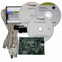
Manufacturer Part Number
MC56F8037EVM
Description
BOARD EVAL FOR MC56F8037
Manufacturer
Freescale Semiconductor
Type
MCUr
Datasheet
1.MC56F8037EVM.pdf
(180 pages)
Specifications of MC56F8037EVM
Contents
Board, Cables, CD, Debugger
Silicon Manufacturer
Freescale
Core Architecture
56800/E
Core Sub-architecture
56800/E
Silicon Core Number
MC56F
Silicon Family Name
MC56F80xx
Kit Contents
MC56F8037EVM, USB-JTAG Adapter, Cables, CD
Rohs Compliant
Yes
For Use With/related Products
MC56F8037
Lead Free Status / RoHS Status
Lead free / RoHS Compliant
Available stocks
Company
Part Number
Manufacturer
Quantity
Price
Company:

Part Number:
MC56F8037EVM
Manufacturer:
Freescale Semiconductor
Quantity:
135


The thermal characterization parameter is measured per JESD51-2 specification using a 40-gauge type T
thermocouple epoxied to the top center of the package case. The thermocouple should be positioned so
that the thermocouple junction rests on the package. A small amount of epoxy is placed over the
thermocouple junction and over about 1mm of wire extending from the junction. The thermocouple wire
is placed flat against the package case to avoid measurement errors caused by cooling effects of the
thermocouple wire.
When heat sink is used, the junction temperature is determined from a thermocouple inserted at the
interface between the case of the package and the interface material. A clearance slot or hole is normally
required in the heat sink. Minimizing the size of the clearance is important to minimize the change in
thermal performance caused by removing part of the thermal interface to the heat sink. Because of the
experimental difficulties with this technique, many engineers measure the heat sink temperature and then
back-calculate the case temperature using a separate measurement of the thermal resistance of the
interface. From this case temperature, the junction temperature is determined from the junction-to-case
thermal resistance.
12.2 Electrical Design Considerations
Use the following list of considerations to assure correct operation of the 56F8037/56F8027:
Freescale Semiconductor
•
•
•
•
•
•
Provide a low-impedance path from the board power supply to each V
from the board ground to each V
The minimum bypass requirement is to place 0.01–0.1µF capacitors positioned as close as possible to the
package supply pins. The recommended bypass configuration is to place one bypass capacitor on each of
the V
tolerances.
Ensure that capacitor leads and associated printed circuit traces that connect to the chip V
pins are as short as possible
Bypass the V
PCB trace lengths should be minimal for high-frequency signals
Consider all device loads as well as parasitic capacitance due to PCB traces when calculating capacitance.
This is especially critical in systems with higher capacitive loads that could create higher transient currents
in the V
DD
DD
/V
SS
and V
DD
pairs, including V
This device contains protective circuitry to guard
against damage due to high static voltage or electrical
fields. However, normal precautions are advised to
avoid
maximum-rated voltages to this high-impedance circuit.
Reliability of operation is enhanced if unused inputs are
tied to an appropriate voltage level.
and V
SS
circuits.
SS
application
with approximately 100µF, plus the number of 0.1µF ceramic capacitors
DDA
56F8037/56F8027 Data Sheet, Rev. 7
SS
(GND) pin
/V
SSA.
of
CAUTION
Ceramic and tantalum capacitors tend to provide better
any
voltages
higher
DD
pin on the 56F8037/56F8027 and
than
Electrical Design Considerations
DD
and V
SS
(GND)
171
Related parts for MC56F8037EVM
Image
Part Number
Description
Manufacturer
Datasheet
Request
R

Part Number:
Description:
Manufacturer:
Freescale Semiconductor, Inc
Datasheet:
Part Number:
Description:
Manufacturer:
Freescale Semiconductor, Inc
Datasheet:
Part Number:
Description:
Manufacturer:
Freescale Semiconductor, Inc
Datasheet:
Part Number:
Description:
Manufacturer:
Freescale Semiconductor, Inc
Datasheet:
Part Number:
Description:
Manufacturer:
Freescale Semiconductor, Inc
Datasheet:
Part Number:
Description:
Manufacturer:
Freescale Semiconductor, Inc
Datasheet:
Part Number:
Description:
Manufacturer:
Freescale Semiconductor, Inc
Datasheet:
Part Number:
Description:
Manufacturer:
Freescale Semiconductor, Inc
Datasheet:
Part Number:
Description:
Manufacturer:
Freescale Semiconductor, Inc
Datasheet:
Part Number:
Description:
Manufacturer:
Freescale Semiconductor, Inc
Datasheet:
Part Number:
Description:
Manufacturer:
Freescale Semiconductor, Inc
Datasheet:
Part Number:
Description:
Manufacturer:
Freescale Semiconductor, Inc
Datasheet:
Part Number:
Description:
Manufacturer:
Freescale Semiconductor, Inc
Datasheet:
Part Number:
Description:
Manufacturer:
Freescale Semiconductor, Inc
Datasheet:
Part Number:
Description:
Manufacturer:
Freescale Semiconductor, Inc
Datasheet: