MC56F8037EVM Freescale Semiconductor, MC56F8037EVM Datasheet - Page 130
MC56F8037EVM
Manufacturer Part Number
MC56F8037EVM
Description
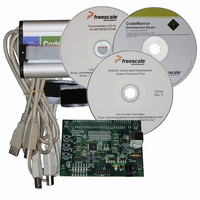
BOARD EVAL FOR MC56F8037
Manufacturer
Freescale Semiconductor
Type
MCUr
Datasheet
1.MC56F8037EVM.pdf
(180 pages)
Specifications of MC56F8037EVM
Contents
Board, Cables, CD, Debugger
Silicon Manufacturer
Freescale
Core Architecture
56800/E
Core Sub-architecture
56800/E
Silicon Core Number
MC56F
Silicon Family Name
MC56F80xx
Kit Contents
MC56F8037EVM, USB-JTAG Adapter, Cables, CD
Rohs Compliant
Yes
For Use With/related Products
MC56F8037
Lead Free Status / RoHS Status
Lead free / RoHS Compliant
Available stocks
Company
Part Number
Manufacturer
Quantity
Price
Company:

Part Number:
MC56F8037EVM
Manufacturer:
Freescale Semiconductor
Quantity:
135


program execution is otherwise unaffected.
7.2 Flash Access Lock and Unlock Mechanisms
There are several methods that effectively lock or unlock the on-chip flash.
7.2.1
On-chip flash can be read by issuing commands across the EOnCE port, which is the debug interface for
the 56800E CPU. The TCK, TMS, TDO, and TDI pins comprise a JTAG interface onto which the EOnCE
port functionality is mapped. When the device boots, the chip-level JTAG TAP (Test Access Port) is active
and provides the chip’s boundary scan capability and access to the ID register, but proper implementation
of flash security will block any attempt to access the internal flash memory via the EOnCE port when
security is enabled.
7.2.2
If the device is secured, one lockout recovery mechanism is the complete erasure of the internal flash
contents, including the configuration field, thus disabling security (the protection register is cleared). This
does not compromise security, as the entire contents of the user’s secured code stored in flash are erased
before security is disabled on the device on the next reset or power-up sequence.
To
(LOCKOUT_RECOVERY) must first be shifted into the chip-level TAP controller’s instruction register.
Once the LOCKOUT_RECOVERY instruction has been shifted into the instruction register, the clock
divider value must be shifted into the corresponding 7-bit data register. After the data register has been
updated, the user must transition the TAP controller into the RUN-TEST/IDLE state for the lockout
sequence to commence. The controller must remain in this state until the erase sequence is complete. Refer
to the 56F802x and 56F803x Peripheral Reference Manual for more details, or contact Freescale.
Note:
7.2.3
CodeWarrior can unlock a device by selecting the Debug menu, then selecting DSP56800E, followed by
Unlock Flash. Another mechanism is also built into CodeWarrior using the device’s memory
configuration file. The command “Unlock_Flash_on_Connect 1” in the .cfg file accomplishes the same
task as using the Debug menu.
This lockout recovery mechanism is the complete erasure of the internal flash contents, including the
configuration field, thus disabling security (the protection register is cleared).
7.2.4
A user can un-secure a secured device by programming the word $0000 into program memory location
$00 7FF7. After completing the programming, both the JTAG TAP controller and the device must be reset
in order to return to normal unsecured operation. Power-on reset will also reset both.
130
start
Disabling EOnCE Access
Flash Lockout Recovery Using JTAG
Once the lockout recovery sequence has completed, the user must reset both the JTAG TAP controller
and device to return to normal unsecured operation. Power-on reset will reset both too.
Flash Lockout Recovery using CodeWarrior
Flash Lockout Recovery without mass erase
the
lockout
recovery
56F8037/56F8027 Data Sheet, Rev. 7
sequence
via
JTAG,
the
JTAG
Freescale Semiconductor
public
instruction
Related parts for MC56F8037EVM
Image
Part Number
Description
Manufacturer
Datasheet
Request
R

Part Number:
Description:
Manufacturer:
Freescale Semiconductor, Inc
Datasheet:
Part Number:
Description:
Manufacturer:
Freescale Semiconductor, Inc
Datasheet:
Part Number:
Description:
Manufacturer:
Freescale Semiconductor, Inc
Datasheet:
Part Number:
Description:
Manufacturer:
Freescale Semiconductor, Inc
Datasheet:
Part Number:
Description:
Manufacturer:
Freescale Semiconductor, Inc
Datasheet:
Part Number:
Description:
Manufacturer:
Freescale Semiconductor, Inc
Datasheet:
Part Number:
Description:
Manufacturer:
Freescale Semiconductor, Inc
Datasheet:
Part Number:
Description:
Manufacturer:
Freescale Semiconductor, Inc
Datasheet:
Part Number:
Description:
Manufacturer:
Freescale Semiconductor, Inc
Datasheet:
Part Number:
Description:
Manufacturer:
Freescale Semiconductor, Inc
Datasheet:
Part Number:
Description:
Manufacturer:
Freescale Semiconductor, Inc
Datasheet:
Part Number:
Description:
Manufacturer:
Freescale Semiconductor, Inc
Datasheet:
Part Number:
Description:
Manufacturer:
Freescale Semiconductor, Inc
Datasheet:
Part Number:
Description:
Manufacturer:
Freescale Semiconductor, Inc
Datasheet:
Part Number:
Description:
Manufacturer:
Freescale Semiconductor, Inc
Datasheet: