MC56F8037EVM Freescale Semiconductor, MC56F8037EVM Datasheet - Page 112
MC56F8037EVM
Manufacturer Part Number
MC56F8037EVM
Description
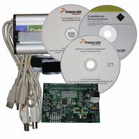
BOARD EVAL FOR MC56F8037
Manufacturer
Freescale Semiconductor
Type
MCUr
Datasheet
1.MC56F8037EVM.pdf
(180 pages)
Specifications of MC56F8037EVM
Contents
Board, Cables, CD, Debugger
Silicon Manufacturer
Freescale
Core Architecture
56800/E
Core Sub-architecture
56800/E
Silicon Core Number
MC56F
Silicon Family Name
MC56F80xx
Kit Contents
MC56F8037EVM, USB-JTAG Adapter, Cables, CD
Rohs Compliant
Yes
For Use With/related Products
MC56F8037
Lead Free Status / RoHS Status
Lead free / RoHS Compliant
Available stocks
Company
Part Number
Manufacturer
Quantity
Price
Company:

Part Number:
MC56F8037EVM
Manufacturer:
Freescale Semiconductor
Quantity:
135


6.3.15.3
These bits enable write protection of GPSn and IPSn registers in the SIM module and write protect all
GPIOx_PEREN, GPIOx_PPOUTM and GPIOx_DRIVE registers in GPIO modules.
Note:
6.3.16
Most I/O pins have an associated GPIO function. In addition to the GPIO function, I/O can be configured
to be one of several peripheral functions. The GPIOx_PEREN register within the GPIO module controls
the selection between peripheral or GPIO control of the I/O pins. The GPIO function is selected when the
GPIOx_PEREN bit for the I/O is 0. When the GPIOx_PEREN bit of the GPIO is 1, the fields in the GPSn
registers select which peripheral function has control of the I/O.
an I/O pin when an I/O has two peripheral functions. Similar muxing is required on peripheral function
inputs to receive input from the properly selected I/O pin.
In some cases, the user can choose peripheral function between several I/O, each of which have the option
to be programmed to control a specific peripheral function. If the user wishes to use that function, only one
of these I/O must be configured to control that peripheral function. If more than one I/O is configured to
control the peripheral function, the peripheral output signal will fan out to each I/O, but the peripheral input
signal will be the logical OR and AND of all the I/O signals.
Complete lists of I/O muxings are provided in
The GPSn setting can be altered during normal operation, but a delay must be inserted between the time
when one function is disabled and another function is enabled.
112
•
•
•
•
•
11 = Write protection on and locked until chip reset
00 = Write protection off (default)
01 = Write protection on
10 = Write protection off and locked until chip reset
11 = Write protection on and locked until chip reset
Figure 6-18 Overall Control of Signal Source Using SIM_GPSnn Control
The PWM fields in the CLKOUT register are also write protected by GIPSP. They are reserved for
in-house test only.
SIM GPIO Peripheral Select Register 0 for GPIOA (SIM_GPSA0)
GPIO and Internal Peripheral Select Protection (GIPSP)—Bits 1–0
Timer A0
FAULT0
PWM
SIM_GPSA0
Register
0
1
56F8037/56F8027 Data Sheet, Rev. 7
Table
2-3.
GPIOA6
GPIOA6_PEREN
Figure 6-18
Register
0
1
GPIOA6 pin
illustrates the output path to
Freescale Semiconductor
Related parts for MC56F8037EVM
Image
Part Number
Description
Manufacturer
Datasheet
Request
R

Part Number:
Description:
Manufacturer:
Freescale Semiconductor, Inc
Datasheet:
Part Number:
Description:
Manufacturer:
Freescale Semiconductor, Inc
Datasheet:
Part Number:
Description:
Manufacturer:
Freescale Semiconductor, Inc
Datasheet:
Part Number:
Description:
Manufacturer:
Freescale Semiconductor, Inc
Datasheet:
Part Number:
Description:
Manufacturer:
Freescale Semiconductor, Inc
Datasheet:
Part Number:
Description:
Manufacturer:
Freescale Semiconductor, Inc
Datasheet:
Part Number:
Description:
Manufacturer:
Freescale Semiconductor, Inc
Datasheet:
Part Number:
Description:
Manufacturer:
Freescale Semiconductor, Inc
Datasheet:
Part Number:
Description:
Manufacturer:
Freescale Semiconductor, Inc
Datasheet:
Part Number:
Description:
Manufacturer:
Freescale Semiconductor, Inc
Datasheet:
Part Number:
Description:
Manufacturer:
Freescale Semiconductor, Inc
Datasheet:
Part Number:
Description:
Manufacturer:
Freescale Semiconductor, Inc
Datasheet:
Part Number:
Description:
Manufacturer:
Freescale Semiconductor, Inc
Datasheet:
Part Number:
Description:
Manufacturer:
Freescale Semiconductor, Inc
Datasheet:
Part Number:
Description:
Manufacturer:
Freescale Semiconductor, Inc
Datasheet: