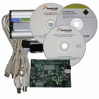
MC56F8037EVM Freescale Semiconductor, MC56F8037EVM Datasheet - Page 172

MC56F8037EVM
Manufacturer Part Number
MC56F8037EVM
Description
BOARD EVAL FOR MC56F8037
Manufacturer
Freescale Semiconductor
Type
MCUr
Datasheet
1.MC56F8037EVM.pdf
(180 pages)
Specifications of MC56F8037EVM
Contents
Board, Cables, CD, Debugger
Silicon Manufacturer
Freescale
Core Architecture
56800/E
Core Sub-architecture
56800/E
Silicon Core Number
MC56F
Silicon Family Name
MC56F80xx
Kit Contents
MC56F8037EVM, USB-JTAG Adapter, Cables, CD
Rohs Compliant
Yes
For Use With/related Products
MC56F8037
Lead Free Status / RoHS Status
Lead free / RoHS Compliant
Available stocks
Company
Part Number
Manufacturer
Quantity
Price
Company:
Part Number:
MC56F8037EVM
Manufacturer:
Freescale Semiconductor
Quantity:
135
- Current page: 172 of 180
- Download datasheet (969Kb)
Part 13 Ordering Information
Table 13-1
sales office or authorized distributor to determine availability and to order devices.
* This package is RoHS compliant.
172
MC56F8037
MC56F8027
MC56F8037
MC56F8027
Device
•
•
•
•
•
•
•
•
•
Take special care to minimize noise levels on the V
Using separate power planes for V
recommended. Connect the separate analog and digital power and ground planes as close as possible to
power supply outputs. If both analog circuit and digital circuit are powered by the same power supply, it is
advisable to connect a small inductor or ferrite bead in serial with both V
It is highly desirable to physically separate analog components from noisy digital components by ground
planes. Do not place an analog trace in parallel with digital traces. It is also desirable to place an analog
ground trace around an analog signal trace to isolate it from digital traces.
Because the Flash memory is programmed through the JTAG/EOnCE port, QSPI, QSCI, or I
designer should provide an interface to this port if in-circuit Flash programming is desired
If desired, connect an external RC circuit to the RESET pin. The Resistor value should be in the range of
4.7k—10k; the Capacitor value should be in the range of 0.22µf - 4.7µf.
Add a 3.3k external pull-up on the TMS pin of the JTAG port to keep EOnce in a restate during normal
operation if JTAG converter is not present
During reset and after reset but before I/O initialization, all I/O pins are at input state with internal pull-up
enable. The typical value of internal pull-up is around 110K. These internal pull-ups can be disabled by
software.
To eliminate PCB trace impedance effect, each ADC input should have a 33pf-10 ohm RC filter
Device GPIOs have only a down (substrate) diode on the GPIO circuit. Devices do not have a positive clamp
diode because GPIOs use a floating gate structure to tolerate 5V input. The absolute maximum clamp
current is -20mA at V
voltage spikes are a concern, a positive clamp is recommended.
lists the pertinent information needed to place an order. Consult a Freescale Semiconductor
3.0–3.6 V
3.0–3.6 V
3.0–3.6 V
3.0–3.6 V
Voltage
Supply
Table 13-1 56F8037/56F8027 Ordering Information
Low-Profile Quad Flat Pack (LQFP)
Low-Profile Quad Flat Pack (LQFP)
Low-Profile Quad Flat Pack (LQFP)
Low-Profile Quad Flat Pack (LQFP)
in
less than 0V. The continuous clamp current is -2mA at V
Package Type
56F8037/56F8027 Data Sheet, Rev. 7
DD
and V
DDA
and separate ground planes for V
Count
REF
Pin
64
64
64
64
, V
DDA
Frequency
(MHz)
, and V
32
32
32
32
SSA
-40° to + 105° C
-40° to + 105° C
-40° to + 125° C
-40° to + 125° C
Temperature
DDA
pins
Ambient
Range
and V
in
SS
less than 0V. If positive
Freescale Semiconductor
SSA
and V
traces.
MC56F8037MLH*
MC56F8027MLH*
MC56F8037VLH*
MC56F8027VLH*
Order Number
SSA
2
C, the
are
Related parts for MC56F8037EVM
Image
Part Number
Description
Manufacturer
Datasheet
Request
R
Part Number:
Description:
Manufacturer:
Freescale Semiconductor, Inc
Datasheet:
Part Number:
Description:
Manufacturer:
Freescale Semiconductor, Inc
Datasheet:
Part Number:
Description:
Manufacturer:
Freescale Semiconductor, Inc
Datasheet:
Part Number:
Description:
Manufacturer:
Freescale Semiconductor, Inc
Datasheet:
Part Number:
Description:
Manufacturer:
Freescale Semiconductor, Inc
Datasheet:
Part Number:
Description:
Manufacturer:
Freescale Semiconductor, Inc
Datasheet:
Part Number:
Description:
Manufacturer:
Freescale Semiconductor, Inc
Datasheet:
Part Number:
Description:
Manufacturer:
Freescale Semiconductor, Inc
Datasheet:
Part Number:
Description:
Manufacturer:
Freescale Semiconductor, Inc
Datasheet:
Part Number:
Description:
Manufacturer:
Freescale Semiconductor, Inc
Datasheet:
Part Number:
Description:
Manufacturer:
Freescale Semiconductor, Inc
Datasheet:
Part Number:
Description:
Manufacturer:
Freescale Semiconductor, Inc
Datasheet:
Part Number:
Description:
Manufacturer:
Freescale Semiconductor, Inc
Datasheet:
Part Number:
Description:
Manufacturer:
Freescale Semiconductor, Inc
Datasheet:
Part Number:
Description:
Manufacturer:
Freescale Semiconductor, Inc
Datasheet:


