MC56F8037EVM Freescale Semiconductor, MC56F8037EVM Datasheet - Page 39
MC56F8037EVM
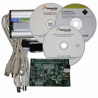
Manufacturer Part Number
MC56F8037EVM
Description
BOARD EVAL FOR MC56F8037
Manufacturer
Freescale Semiconductor
Type
MCUr
Datasheet
1.MC56F8037EVM.pdf
(180 pages)
Specifications of MC56F8037EVM
Contents
Board, Cables, CD, Debugger
Silicon Manufacturer
Freescale
Core Architecture
56800/E
Core Sub-architecture
56800/E
Silicon Core Number
MC56F
Silicon Family Name
MC56F80xx
Kit Contents
MC56F8037EVM, USB-JTAG Adapter, Cables, CD
Rohs Compliant
Yes
For Use With/related Products
MC56F8037
Lead Free Status / RoHS Status
Lead free / RoHS Compliant
Available stocks
Company
Part Number
Manufacturer
Quantity
Price
Company:

Part Number:
MC56F8037EVM
Manufacturer:
Freescale Semiconductor
Quantity:
135


Freescale Semiconductor
Table 2-3 56F8037/56F8027 Signal and Package Information for the 64-Pin LQFP (Continued)
Return to
(GPIOD0)
(GPIOD1)
GPIOD5
(CLKIN)
GPIOD6
GPIOD7
(DAC0)
(DAC1)
(XTAL)
Signal
Name
TDO
TDI
Table 2-2
Pin No.
LQFP
52
18
15
59
64
Analog
Analog
Analog
Output
Output
Output
Output
Output
Output
Output
Input/
Input/
Input/
Input/
Input/
Input/
Type
Input
Input
Input
Input
State During
tri-stated,
enabled
enabled
enabled
enabled
internal
internal
internal
internal
pull-up
pull-up
pull-up
Output
pull-up
Reset
Input,
Input,
Input,
56F8037/56F8027 Data Sheet, Rev. 7
Input
Port D GPIO — This GPIO pin can be individually programmed as
an input or output pin.
External Crystal Oscillator Output — This output connects the
internal crystal oscillator output to an external crystal.
External Clock Input — This pin serves as an external clock input.
After reset, the default state is GPIOD5.
Port D GPIO — This GPIO pin can be individually programmed as
an input or output pin.
DAC0— Digital-to-Analog Converter output 0.
After reset, the default state is GPIOD6.
Port D GPIO — This GPIO pin can be individually programmed as
an input or output pin.
DAC1— Digital-to-Analog Converter output 1.
After reset, the default state is GPIOD7.
Test Data Input — This input pin provides a serial input data stream
to the JTAG/EOnCE port. It is sampled on the rising edge of TCK
and has an on-chip pull-up resistor.
Port D GPIO — This GPIO pin can be individually programmed as
an input or output pin.
After reset, the default state is TDI.
Test Data Output — This tri-stateable output pin provides a serial
output data stream from the JTAG/EOnCE port. It is driven in the
shift-IR and shift-DR controller states, and changes on the falling
edge of TCK.
Port D GPIO — This GPIO pin can be individually programmed as
an input or output pin.
After reset, the default state is TDO.
Signal Description
56F8037/56F8027 Signal Pins
39
Related parts for MC56F8037EVM
Image
Part Number
Description
Manufacturer
Datasheet
Request
R

Part Number:
Description:
Manufacturer:
Freescale Semiconductor, Inc
Datasheet:
Part Number:
Description:
Manufacturer:
Freescale Semiconductor, Inc
Datasheet:
Part Number:
Description:
Manufacturer:
Freescale Semiconductor, Inc
Datasheet:
Part Number:
Description:
Manufacturer:
Freescale Semiconductor, Inc
Datasheet:
Part Number:
Description:
Manufacturer:
Freescale Semiconductor, Inc
Datasheet:
Part Number:
Description:
Manufacturer:
Freescale Semiconductor, Inc
Datasheet:
Part Number:
Description:
Manufacturer:
Freescale Semiconductor, Inc
Datasheet:
Part Number:
Description:
Manufacturer:
Freescale Semiconductor, Inc
Datasheet:
Part Number:
Description:
Manufacturer:
Freescale Semiconductor, Inc
Datasheet:
Part Number:
Description:
Manufacturer:
Freescale Semiconductor, Inc
Datasheet:
Part Number:
Description:
Manufacturer:
Freescale Semiconductor, Inc
Datasheet:
Part Number:
Description:
Manufacturer:
Freescale Semiconductor, Inc
Datasheet:
Part Number:
Description:
Manufacturer:
Freescale Semiconductor, Inc
Datasheet:
Part Number:
Description:
Manufacturer:
Freescale Semiconductor, Inc
Datasheet:
Part Number:
Description:
Manufacturer:
Freescale Semiconductor, Inc
Datasheet: