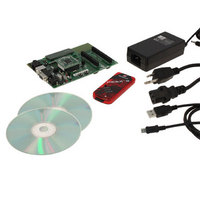
DV164136 Microchip Technology, DV164136 Datasheet - Page 101

DV164136
Manufacturer Part Number
DV164136
Description
DEVELOPMENT KIT FOR PIC18
Manufacturer
Microchip Technology
Series
PIC®r
Type
MCUr
Datasheets
1.DM183032.pdf
(38 pages)
2.DV164136.pdf
(448 pages)
3.DV164136.pdf
(6 pages)
4.DV164136.pdf
(446 pages)
5.DV164136.pdf
(4 pages)
6.DV164136.pdf
(18 pages)
Specifications of DV164136
Contents
Board, Cables, CDs, PICkit™ 3 Programmer, Power Supply
Processor To Be Evaluated
PIC18F8722, PIC18F87J11
Interface Type
RS-232, USB
Operating Supply Voltage
3.3 V, 5 V
Silicon Manufacturer
Microchip
Core Architecture
PIC
Core Sub-architecture
PIC18
Silicon Core Number
PIC18F
Silicon Family Name
PIC18F8xxx
Kit Contents
PIC18 Exp Brd PICkit 3 Cable CD PSU
Lead Free Status / RoHS Status
Lead free / RoHS Compliant
For Use With/related Products
PIC18F8722, PIC18F87J11
Lead Free Status / Rohs Status
Lead free / RoHS Compliant
Available stocks
Company
Part Number
Manufacturer
Quantity
Price
Company:
Part Number:
DV164136
Manufacturer:
MICROCHIP
Quantity:
12 000
- DM183032 PDF datasheet
- DV164136 PDF datasheet #2
- DV164136 PDF datasheet #3
- DV164136 PDF datasheet #4
- DV164136 PDF datasheet #5
- DV164136 PDF datasheet #6
- Current page: 101 of 446
- Download datasheet (7Mb)
7.2
PIC18F8527/8622/8627/8722 devices can be indepen-
dently configured for different address and data widths
on the same memory bus. Both address and data width
are set by Configuration bits in the CONFIG3L register.
As Configuration bits, this means that these options
can only be configured by programming the device and
are not controllable in software.
The BW bit selects an 8-bit or 16-bit data bus width.
Setting this bit (default) selects a data width of 16 bits.
The ADW<1:0> bits determine the address bus width.
The available options are 20-bit (default), 16-bit, 12-bit
and 8-bit. Selecting any of the options other than 20-bit
width makes a corresponding number of high-order
lines available for I/O functions; these pins are no
longer affected by the setting of the EBDIS bit. For
example,
(ADW<1:0> = 10) disables A<19:16> and allows
PORTH<3:0> to function without interruptions from the
bus. Using smaller address widths allows users to tailor
the memory bus to the size of the external memory
space for a particular design while freeing up pins for
dedicated I/O operation.
Because the ADW bits have the effect of disabling pins
for memory bus operations, it is important to always
select an address width at least equal to the data width.
If 8-bit or 12-bit address widths are used with a 16-bit
data width, the upper bits of data will not be available
on the bus.
All combinations of address and data widths require
multiplexing of address and data information on the
same lines. The address and data multiplexing, as well
as I/O ports made available by the use of smaller
address widths, are summarized in Table 7-2.
TABLE 7-2:
© 2008 Microchip Technology Inc.
Data Width
16-bit
8-bit
Address and Data Width
selecting
ADDRESS AND DATA LINES FOR DIFFERENT ADDRESS AND DATA WIDTHS
a
Address Width
16-bit
12-bit
16-bit
20-bit
16-bit
20-bit
8-bit
Address
Corresponding Ports)
Multiplexed Data and
Address Lines (and
mode
(PORTD<7:0>)
(PORTD<7:0>,
PORTE<7:0>)
AD<15:0>
AD<7:0>
7.2.1
As an extension of 20-bit address width operation, the
External Memory Bus can also fully address a 2 Mbyte
memory space. This is done by using the Bus Address
bit 0 (BA0) control line as the Least Significant bit of the
address. The UB and LB control signals may also be
used with certain memory devices to select the upper
and lower bytes within a 16-bit wide data word.
This addressing mode is available in both 8-bit and
certain 16-bit Data Width modes. Additional details are
provided in Section 7.5.3 “16-bit Byte Select Mode”
and Section 7.6 “8-Bit Data Width Modes”.
7.3
While it may be assumed that external memory devices
will operate at the microcontroller clock rate, this is
often not the case. In fact, many devices require longer
times to write or retrieve data than the time allowed by
the execution of table read or table write operations.
To compensate for this, the External Memory Bus can
be configured to add a fixed delay to each table opera-
tion using the bus. Wait states are enabled by setting
the WAITx bit. When enabled, the amount of delay is
set by the WAIT<1:0> bits (MEMCON<5:4>). The delay
is based on multiples of microcontroller instruction
cycle time and are added following the instruction cycle
when the table operation is executed. The range is
from no delay to 3 T
PIC18F8722 FAMILY
Corresponding Ports)
A<19:16>, AD<15:8>
Wait States
(PORTE<3:0>)
(PORTE<7:0>)
(PORTH<3:0>,
(PORTH<3:0>)
Address-Only
21-BIT ADDRESSING
PORTE<7:0>)
Lines (and
AD<11:8>
AD<15:8>
A<19:16>
—
—
CY
(default value).
All of PORTE and
Ports Available
PORTE<7:4>,
All of PORTH
All of PORTH
All of PORTH
DS39646C-page 99
PORTH
for I/O
—
—
Related parts for DV164136
Image
Part Number
Description
Manufacturer
Datasheet
Request
R

Part Number:
Description:
Manufacturer:
Microchip Technology Inc.
Datasheet:

Part Number:
Description:
Manufacturer:
Microchip Technology Inc.
Datasheet:

Part Number:
Description:
Manufacturer:
Microchip Technology Inc.
Datasheet:

Part Number:
Description:
Manufacturer:
Microchip Technology Inc.
Datasheet:

Part Number:
Description:
Manufacturer:
Microchip Technology Inc.
Datasheet:

Part Number:
Description:
Manufacturer:
Microchip Technology Inc.
Datasheet:

Part Number:
Description:
Manufacturer:
Microchip Technology Inc.
Datasheet:

Part Number:
Description:
Manufacturer:
Microchip Technology Inc.
Datasheet:


