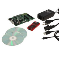
DV164136 Microchip Technology, DV164136 Datasheet - Page 276

DV164136
Manufacturer Part Number
DV164136
Description
DEVELOPMENT KIT FOR PIC18
Manufacturer
Microchip Technology
Series
PIC®r
Type
MCUr
Datasheets
1.DM183032.pdf
(38 pages)
2.DV164136.pdf
(448 pages)
3.DV164136.pdf
(6 pages)
4.DV164136.pdf
(446 pages)
5.DV164136.pdf
(4 pages)
6.DV164136.pdf
(18 pages)
Specifications of DV164136
Contents
Board, Cables, CDs, PICkit™ 3 Programmer, Power Supply
Processor To Be Evaluated
PIC18F8722, PIC18F87J11
Interface Type
RS-232, USB
Operating Supply Voltage
3.3 V, 5 V
Silicon Manufacturer
Microchip
Core Architecture
PIC
Core Sub-architecture
PIC18
Silicon Core Number
PIC18F
Silicon Family Name
PIC18F8xxx
Kit Contents
PIC18 Exp Brd PICkit 3 Cable CD PSU
Lead Free Status / RoHS Status
Lead free / RoHS Compliant
For Use With/related Products
PIC18F8722, PIC18F87J11
Lead Free Status / Rohs Status
Lead free / RoHS Compliant
Available stocks
Company
Part Number
Manufacturer
Quantity
Price
Company:
Part Number:
DV164136
Manufacturer:
MICROCHIP
Quantity:
12 000
- DM183032 PDF datasheet
- DV164136 PDF datasheet #2
- DV164136 PDF datasheet #3
- DV164136 PDF datasheet #4
- DV164136 PDF datasheet #5
- DV164136 PDF datasheet #6
- Current page: 276 of 446
- Download datasheet (7Mb)
PIC18F8722 FAMILY
The analog reference voltage is software selectable to
either the device’s positive and negative supply voltage
(V
V
The A/D converter has a unique feature of being able
to operate while the device is in Sleep mode. To oper-
ate in Sleep, the A/D conversion clock must be derived
from the A/D’s internal RC oscillator.
The output of the sample and hold is the input into the
converter, which generates the result via successive
approximation.
FIGURE 21-1:
DS39646C-page 274
REF
DD
+ and RA2/AN2/V
and V
Note 1:
SS
2:
), or the voltage level on the RA3/AN3/
Converter
10-Bit
Channels AN12 through AN15 are not available on 64-pin devices.
I/O pins have diode protection to V
A/D
Reference
Voltage
A/D BLOCK DIAGRAM
REF
- pins.
V
V
REF
REF
+
-
(Input Voltage)
VCFG<1:0>
V
AIN
DD
and V
X
X
1
0
0
1
X
X
AV
SS
A device Reset forces all registers to their Reset state.
This forces the A/D module to be turned off and any
conversion in progress is aborted.
Each port pin associated with the A/D converter can be
configured as an analog input, or as a digital I/O. The
ADRESH and ADRESL registers contain the result of
the A/D conversion. When the A/D conversion is com-
plete, the result is loaded into the ADRESH:ADRESL
register pair, the GO/DONE bit (ADCON0 register) is
cleared and A/D Interrupt Flag bit, ADIF (PIR1<6>), is
set. The block diagram of the A/D module is shown in
Figure 21-1.
.
DD
AV
SS
CHS<3:0>
1111
1110
1101
1100
1011
1010
1001
1000
0111
0110
0101
0100
0011
0010
0001
0000
© 2008 Microchip Technology Inc.
AN15
AN14
AN13
AN12
AN11
AN10
AN9
AN8
AN7
AN6
AN5
AN4
AN3
AN2
AN1
AN0
(1)
(1)
(1)
(1)
Related parts for DV164136
Image
Part Number
Description
Manufacturer
Datasheet
Request
R

Part Number:
Description:
Manufacturer:
Microchip Technology Inc.
Datasheet:

Part Number:
Description:
Manufacturer:
Microchip Technology Inc.
Datasheet:

Part Number:
Description:
Manufacturer:
Microchip Technology Inc.
Datasheet:

Part Number:
Description:
Manufacturer:
Microchip Technology Inc.
Datasheet:

Part Number:
Description:
Manufacturer:
Microchip Technology Inc.
Datasheet:

Part Number:
Description:
Manufacturer:
Microchip Technology Inc.
Datasheet:

Part Number:
Description:
Manufacturer:
Microchip Technology Inc.
Datasheet:

Part Number:
Description:
Manufacturer:
Microchip Technology Inc.
Datasheet:


