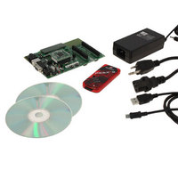
DV164136 Microchip Technology, DV164136 Datasheet - Page 280

DV164136
Manufacturer Part Number
DV164136
Description
DEVELOPMENT KIT FOR PIC18
Manufacturer
Microchip Technology
Series
PIC®r
Type
MCUr
Datasheets
1.DM183032.pdf
(38 pages)
2.DV164136.pdf
(448 pages)
3.DV164136.pdf
(6 pages)
4.DV164136.pdf
(446 pages)
5.DV164136.pdf
(4 pages)
6.DV164136.pdf
(18 pages)
Specifications of DV164136
Contents
Board, Cables, CDs, PICkit™ 3 Programmer, Power Supply
Processor To Be Evaluated
PIC18F8722, PIC18F87J11
Interface Type
RS-232, USB
Operating Supply Voltage
3.3 V, 5 V
Silicon Manufacturer
Microchip
Core Architecture
PIC
Core Sub-architecture
PIC18
Silicon Core Number
PIC18F
Silicon Family Name
PIC18F8xxx
Kit Contents
PIC18 Exp Brd PICkit 3 Cable CD PSU
Lead Free Status / RoHS Status
Lead free / RoHS Compliant
For Use With/related Products
PIC18F8722, PIC18F87J11
Lead Free Status / Rohs Status
Lead free / RoHS Compliant
Available stocks
Company
Part Number
Manufacturer
Quantity
Price
Company:
Part Number:
DV164136
Manufacturer:
MICROCHIP
Quantity:
12 000
- DM183032 PDF datasheet
- DV164136 PDF datasheet #2
- DV164136 PDF datasheet #3
- DV164136 PDF datasheet #4
- DV164136 PDF datasheet #5
- DV164136 PDF datasheet #6
- Current page: 280 of 446
- Download datasheet (7Mb)
PIC18F8722 FAMILY
21.4
The selection of the automatic acquisition time and A/D
conversion clock is determined in part by the clock
source and frequency while in a power-managed mode.
If the A/D is expected to operate while the device is in
a power-managed mode, the ACQT<2:0> and
ADCS<2:0> bits in ADCON2 should be updated in
accordance with the clock source to be used in that
mode. After entering the mode, an A/D acquisition or
conversion may be started. Once started, the device
should continue to be clocked by the same clock
source until the conversion has been completed.
If desired, the device may be placed into the
corresponding Idle mode during the conversion. If the
device clock frequency is less than 1 MHz, the A/D RC
clock source should be selected.
Operation in the Sleep mode requires the A/D F
clock to be selected. If bits ACQT<2:0> are set to ‘000’
and a conversion is started, the conversion will be
delayed one instruction cycle to allow execution of the
SLEEP instruction and entry to Sleep mode. The IDLEN
bit (OSCCON<7>) must have already been cleared
prior to starting the conversion.
DS39646C-page 278
Operation in Power-Managed
Modes
RC
21.5
The ADCON1, TRISA, TRISF and TRISH registers all
configure the A/D port pins. The port pins needed as
analog inputs must have their corresponding TRIS bits
set (input). If the TRIS bit is cleared (output), the digital
output level (V
The A/D operation is independent of the state of the
CHS<3:0> bits and the TRIS bits.
Note 1: When reading the Port register, all pins
2: Analog levels on any pin defined as a
Configuring Analog Port Pins
configured as analog input channels will
read as cleared (a low level). Pins con-
figured as digital inputs will convert as
analog inputs. Analog levels on a digitally
configured
converted.
digital input may cause the digital input
buffer to consume current out of the
device’s specification limits.
OH
or V
OL
© 2008 Microchip Technology Inc.
) will be converted.
input
will
be
accurately
Related parts for DV164136
Image
Part Number
Description
Manufacturer
Datasheet
Request
R

Part Number:
Description:
Manufacturer:
Microchip Technology Inc.
Datasheet:

Part Number:
Description:
Manufacturer:
Microchip Technology Inc.
Datasheet:

Part Number:
Description:
Manufacturer:
Microchip Technology Inc.
Datasheet:

Part Number:
Description:
Manufacturer:
Microchip Technology Inc.
Datasheet:

Part Number:
Description:
Manufacturer:
Microchip Technology Inc.
Datasheet:

Part Number:
Description:
Manufacturer:
Microchip Technology Inc.
Datasheet:

Part Number:
Description:
Manufacturer:
Microchip Technology Inc.
Datasheet:

Part Number:
Description:
Manufacturer:
Microchip Technology Inc.
Datasheet:


