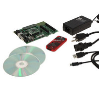
DV164136 Microchip Technology, DV164136 Datasheet - Page 282

DV164136
Manufacturer Part Number
DV164136
Description
DEVELOPMENT KIT FOR PIC18
Manufacturer
Microchip Technology
Series
PIC®r
Type
MCUr
Datasheets
1.DM183032.pdf
(38 pages)
2.DV164136.pdf
(448 pages)
3.DV164136.pdf
(6 pages)
4.DV164136.pdf
(446 pages)
5.DV164136.pdf
(4 pages)
6.DV164136.pdf
(18 pages)
Specifications of DV164136
Contents
Board, Cables, CDs, PICkit™ 3 Programmer, Power Supply
Processor To Be Evaluated
PIC18F8722, PIC18F87J11
Interface Type
RS-232, USB
Operating Supply Voltage
3.3 V, 5 V
Silicon Manufacturer
Microchip
Core Architecture
PIC
Core Sub-architecture
PIC18
Silicon Core Number
PIC18F
Silicon Family Name
PIC18F8xxx
Kit Contents
PIC18 Exp Brd PICkit 3 Cable CD PSU
Lead Free Status / RoHS Status
Lead free / RoHS Compliant
For Use With/related Products
PIC18F8722, PIC18F87J11
Lead Free Status / Rohs Status
Lead free / RoHS Compliant
Available stocks
Company
Part Number
Manufacturer
Quantity
Price
Company:
Part Number:
DV164136
Manufacturer:
MICROCHIP
Quantity:
12 000
- DM183032 PDF datasheet
- DV164136 PDF datasheet #2
- DV164136 PDF datasheet #3
- DV164136 PDF datasheet #4
- DV164136 PDF datasheet #5
- DV164136 PDF datasheet #6
- Current page: 282 of 446
- Download datasheet (7Mb)
PIC18F8722 FAMILY
21.8
An A/D conversion can be started by the Special Event
Trigger of the ECCP2 module. This requires that the
CCP2M<3:0> bits (CCP2CON<3:0>) be programmed
as ‘1011’ and that the A/D module is enabled (ADON
bit is set). When the trigger occurs, the GO/DONE bit
will be set, starting the A/D acquisition and conversion
and the Timer1 (or Timer3) counter will be reset to zero.
Timer1 (or Timer3) is reset to automatically repeat the
A/D acquisition period with minimal software overhead
TABLE 21-2:
DS39646C-page 280
INTCON
PIR1
PIE1
IPR1
PIR2
PIE2
IPR2
ADRESH
ADRESL
ADCON0
ADCON1
ADCON2
TRISA
TRISF
TRISH
Legend: — = unimplemented, read as ‘0’. Shaded cells are not used for A/D conversion.
Note 1:
Name
2:
(2)
Use of the ECCP2 Trigger
PORTA<7:6> and their direction bits are individually configured as port pins based on various primary
oscillator modes. When disabled, these bits read as ‘0’.
These registers are not implemented on 64-pin devices.
GIE/GIEH PEIE/GIEL TMR0IE
A/D Result Register High Byte
A/D Result Register Low Byte
TRISA7
OSCFIF
OSCFIE
OSCFIP
TRISH7
TRISF7
PSPIF
PSPIE
PSPIP
ADFM
Bit 7
—
—
REGISTERS ASSOCIATED WITH A/D OPERATION
(1)
TRISA6
TRISH6
TRISF6
CMIE
CMIP
CMIF
ADIF
ADIE
ADIP
Bit 6
—
—
—
(1)
TRISA5
TRISH5
VCFG1
ACQT2
TRISF5
RC1IE
RC1IP
RC1IF
CHS3
Bit 5
—
—
—
TRISH4
TRISA4
TRISF4
VCFG0
ACQT1
INT0IE
TX1IE
TX1IP
TX1IF
CHS2
EEIF
EEIE
EEIP
Bit 4
TRISH3
SSP1IF
SSP1IE
SSP1IP
BCL1IF
BCL1IE
BCL1IP
TRISA3
TRISF3
PCFG3
ACQT0
CHS1
(moving ADRESH:ADRESL to the desired location).
The appropriate analog input channel must be selected
and the minimum acquisition period is either timed by
the user, or an appropriate T
the Special Event Trigger sets the GO/DONE bit (starts
a conversion).
If the A/D module is not enabled (ADON is cleared), the
Special Event Trigger will be ignored by the A/D module
but will still reset the Timer1 (or Timer3) counter.
RBIE
Bit 3
TMR0IF
CCP1IF
CCP1IE
CCP1IP
TRISH2
HLVDIF
HLVDIE
HLVDIP
TRISA2
TRISF2
PCFG2
ADCS2
CHS0
Bit 2
GO/DONE
TMR2IF
TMR2IE
TMR2IP
TMR3IF
TMR3IE
TMR3IP
TRISH1
TRISA1
TRISF1
PCFG1
ADCS1
INT0IF
Bit 1
© 2008 Microchip Technology Inc.
ACQ
time selected before
TMR1IF
TMR1IE
TMR1IP
CCP2IF
CCP2IE
CCP2IP
TRISH0
TRISA0
TRISF0
PCFG0
ADCS0
ADON
RBIF
Bit 0
on page
Values
Reset
57
60
60
60
60
60
60
59
59
59
59
59
60
60
60
Related parts for DV164136
Image
Part Number
Description
Manufacturer
Datasheet
Request
R

Part Number:
Description:
Manufacturer:
Microchip Technology Inc.
Datasheet:

Part Number:
Description:
Manufacturer:
Microchip Technology Inc.
Datasheet:

Part Number:
Description:
Manufacturer:
Microchip Technology Inc.
Datasheet:

Part Number:
Description:
Manufacturer:
Microchip Technology Inc.
Datasheet:

Part Number:
Description:
Manufacturer:
Microchip Technology Inc.
Datasheet:

Part Number:
Description:
Manufacturer:
Microchip Technology Inc.
Datasheet:

Part Number:
Description:
Manufacturer:
Microchip Technology Inc.
Datasheet:

Part Number:
Description:
Manufacturer:
Microchip Technology Inc.
Datasheet:


