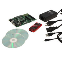
DV164136 Microchip Technology, DV164136 Datasheet - Page 322

DV164136
Manufacturer Part Number
DV164136
Description
DEVELOPMENT KIT FOR PIC18
Manufacturer
Microchip Technology
Series
PIC®r
Type
MCUr
Datasheets
1.DM183032.pdf
(38 pages)
2.DV164136.pdf
(448 pages)
3.DV164136.pdf
(6 pages)
4.DV164136.pdf
(446 pages)
5.DV164136.pdf
(4 pages)
6.DV164136.pdf
(18 pages)
Specifications of DV164136
Contents
Board, Cables, CDs, PICkit™ 3 Programmer, Power Supply
Processor To Be Evaluated
PIC18F8722, PIC18F87J11
Interface Type
RS-232, USB
Operating Supply Voltage
3.3 V, 5 V
Silicon Manufacturer
Microchip
Core Architecture
PIC
Core Sub-architecture
PIC18
Silicon Core Number
PIC18F
Silicon Family Name
PIC18F8xxx
Kit Contents
PIC18 Exp Brd PICkit 3 Cable CD PSU
Lead Free Status / RoHS Status
Lead free / RoHS Compliant
For Use With/related Products
PIC18F8722, PIC18F87J11
Lead Free Status / Rohs Status
Lead free / RoHS Compliant
Available stocks
Company
Part Number
Manufacturer
Quantity
Price
Company:
Part Number:
DV164136
Manufacturer:
MICROCHIP
Quantity:
12 000
- DM183032 PDF datasheet
- DV164136 PDF datasheet #2
- DV164136 PDF datasheet #3
- DV164136 PDF datasheet #4
- DV164136 PDF datasheet #5
- DV164136 PDF datasheet #6
- Current page: 322 of 446
- Download datasheet (7Mb)
PIC18F8722 FAMILY
25.5.2
The entire data EEPROM is protected from external
reads and writes by two bits: CPD and WRTD. CPD
inhibits external reads and writes of data EEPROM.
WRTD inhibits internal and external writes to data
EEPROM. The CPU can always read data EEPROM
under normal operation, regardless of the protection bit
settings.
25.5.3
The Configuration registers can be write-protected.
The WRTC bit controls protection of the Configuration
registers. In normal execution mode, the WRTC bit is
readable only. WRTC can only be written via ICSP or
an external programmer.
25.6
Eight memory locations (200000h-200007h) are
designated as ID locations, where the user can store
checksum or other code identification numbers. These
locations are both readable and writable during normal
execution through the TBLRD and TBLWT instructions
or during program/verify. The ID locations can be read
when the device is code-protected.
25.7
The PIC18F8722 family of devices can be serially
programmed while in the end application circuit. This is
simply done with two lines for clock and data and three
other lines for power, ground and the programming
voltage. This allows customers to manufacture boards
with unprogrammed devices and then program the
microcontroller just before shipping the product. This
also allows the most recent firmware or a custom
firmware to be programmed.
25.8
When the DEBUG Configuration bit is programmed to
a ‘0’, the In-Circuit Debugger functionality is enabled.
This function allows simple debugging functions when
used with MPLAB
this feature enabled, some resources are not available
for general use. Table 25-4 shows which resources are
required by the background debugger.
TABLE 25-4:
DS39646C-page 320
I/O pins:
Stack:
Program Memory:
Data Memory:
ID Locations
In-Circuit Debugger
In-Circuit Serial Programming
DATA EEPROM
CODE PROTECTION
CONFIGURATION REGISTER
PROTECTION
®
DEBUGGER RESOURCES
IDE. When the microcontroller has
RB6, RB7
2 levels
512 bytes
10 bytes
To use the In-Circuit Debugger function of the micro-
controller, the design must implement In-Circuit Serial
Programming connections to RG5/MCLR/V
V
Debugger module available from Microchip or one of
the third party development tool companies.
25.9
The LVP Configuration bit enables Single-Supply ICSP
Programming (formerly known as Low-Voltage ICSP
Programming or LVP). When Single-Supply Program-
ming is enabled, the microcontroller can be programmed
without requiring high voltage being applied to the
RG5/MCLR/V
dedicated to controlling Program mode entry and is not
available as a general purpose I/O pin.
While programming, using single-supply programming
mode, V
normal execution mode. To enter Programming mode,
V
If Single-Supply ICSP Programming mode will not be
used, the LVP bit can be cleared. RB5/KBI1/PGM then
becomes available as the digital I/O pin, RB5. The LVP
bit may be set or cleared only when using standard
high-voltage programming (V
MCLR/V
standard high-voltage programming is available and
must be used to program the device.
Memory that is not code-protected can be erased using
a block erase, or erased row by row, then written at any
specified V
erased, a block erase is required. If a block erase is to
be performed when using Low-Voltage Programming,
the device must be supplied with V
DD
SS
Note 1: High-voltage programming is always
, RB7 and RB6. This will interface to the In-Circuit
is applied to the PGM pin.
DD
PP
2: By
3: When Single-Supply Programming is
4: When LVP is enabled, externally pull the
Single-Supply ICSP Programming
pin). Once LVP has been disabled, only the
is applied to the RG5/MCLR/V
DD
available, regardless of the state of the
LVP bit or the PGM pin, by applying V
to the MCLR pin.
enabled in unprogrammed devices (as
supplied from Microchip) and erased
devices.
enabled, the RB5 pin can no longer be
used as a general purpose I/O pin.
PGM pin to V
execution.
PP
. If code-protected memory is to be
pin, but the RB5/KBI1/PGM pin is then
default,
© 2008 Microchip Technology Inc.
SS
Single-Supply
to allow normal program
IHH
applied to the RG5/
DD
of 4.5V to 5.5V.
PP
ICSP
PP
pin as in
, V
IHH
DD
is
,
Related parts for DV164136
Image
Part Number
Description
Manufacturer
Datasheet
Request
R

Part Number:
Description:
Manufacturer:
Microchip Technology Inc.
Datasheet:

Part Number:
Description:
Manufacturer:
Microchip Technology Inc.
Datasheet:

Part Number:
Description:
Manufacturer:
Microchip Technology Inc.
Datasheet:

Part Number:
Description:
Manufacturer:
Microchip Technology Inc.
Datasheet:

Part Number:
Description:
Manufacturer:
Microchip Technology Inc.
Datasheet:

Part Number:
Description:
Manufacturer:
Microchip Technology Inc.
Datasheet:

Part Number:
Description:
Manufacturer:
Microchip Technology Inc.
Datasheet:

Part Number:
Description:
Manufacturer:
Microchip Technology Inc.
Datasheet:


