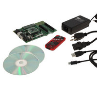
DV164136 Microchip Technology, DV164136 Datasheet - Page 345

DV164136
Manufacturer Part Number
DV164136
Description
DEVELOPMENT KIT FOR PIC18
Manufacturer
Microchip Technology
Series
PIC®r
Type
MCUr
Datasheets
1.DM183032.pdf
(38 pages)
2.DV164136.pdf
(448 pages)
3.DV164136.pdf
(6 pages)
4.DV164136.pdf
(446 pages)
5.DV164136.pdf
(4 pages)
6.DV164136.pdf
(18 pages)
Specifications of DV164136
Contents
Board, Cables, CDs, PICkit™ 3 Programmer, Power Supply
Processor To Be Evaluated
PIC18F8722, PIC18F87J11
Interface Type
RS-232, USB
Operating Supply Voltage
3.3 V, 5 V
Silicon Manufacturer
Microchip
Core Architecture
PIC
Core Sub-architecture
PIC18
Silicon Core Number
PIC18F
Silicon Family Name
PIC18F8xxx
Kit Contents
PIC18 Exp Brd PICkit 3 Cable CD PSU
Lead Free Status / RoHS Status
Lead free / RoHS Compliant
For Use With/related Products
PIC18F8722, PIC18F87J11
Lead Free Status / Rohs Status
Lead free / RoHS Compliant
Available stocks
Company
Part Number
Manufacturer
Quantity
Price
Company:
Part Number:
DV164136
Manufacturer:
MICROCHIP
Quantity:
12 000
- DM183032 PDF datasheet
- DV164136 PDF datasheet #2
- DV164136 PDF datasheet #3
- DV164136 PDF datasheet #4
- DV164136 PDF datasheet #5
- DV164136 PDF datasheet #6
- Current page: 345 of 446
- Download datasheet (7Mb)
INCFSZ
Syntax:
Operands:
Operation:
Status Affected:
Encoding:
Description:
Words:
Cycles:
Example:
© 2008 Microchip Technology Inc.
Q Cycle Activity:
If skip:
If skip and followed by 2-word instruction:
Before Instruction
After Instruction
operation
operation
operation
Decode
No
No
No
PC
CNT
If CNT
PC
If CNT
PC
Q1
Q1
Q1
=
=
=
=
≠
=
register ‘f’
operation
operation
operation
Increment f, Skip if 0
INCFSZ
0 ≤ f ≤ 255
d ∈ [0,1]
a ∈ [0,1]
(f) + 1 → dest,
skip if result = 0
None
The contents of register ‘f’ are
incremented. If ‘d’ is ‘0’, the result is
placed in W. If ‘d’ is ‘1’, the result is
placed back in register ‘f’. (default)
If the result is ‘0’, the next instruction
which is already fetched is discarded
and a NOP is executed instead, making
it a two-cycle instruction.
If ‘a’ is ‘0’, the Access Bank is selected.
If ‘a’ is ‘1’, the BSR is used to select the
GPR bank (default).
If ‘a’ is ‘0’ and the extended instruction
set is enabled, this instruction operates
in Indexed Literal Offset Addressing
mode whenever f ≤ 95 (5Fh). See
Section 26.2.3 “Byte-Oriented and
Bit-Oriented Instructions in Indexed
Literal Offset Mode” for details.
1
1(2)
Note:
HERE
NZERO
ZERO
Read
0011
No
No
No
Q2
Q2
Q2
Address (HERE)
CNT + 1
0;
Address (ZERO)
0;
Address (NZERO)
3 cycles if skip and followed
by a 2-word instruction.
f {,d {,a}}
INCFSZ
:
:
11da
operation
operation
operation
Process
Data
No
No
No
Q3
Q3
Q3
ffff
CNT, 1, 0
destination
operation
operation
operation
Write to
No
No
No
Q4
Q4
Q4
ffff
INFSNZ
Syntax:
Operands:
Operation:
Status Affected:
Encoding:
Description:
Words:
Cycles:
Example:
Q Cycle Activity:
If skip:
If skip and followed by 2-word instruction:
PIC18F8722 FAMILY
Before Instruction
After Instruction
operation
operation
operation
Decode
No
No
No
PC
REG
If REG
PC
If REG
PC
Q1
Q1
Q1
=
=
≠
=
=
=
register ‘f’
operation
operation
operation
Increment f, Skip if not 0
INFSNZ
0 ≤ f ≤ 255
d ∈ [0,1]
a ∈ [0,1]
(f) + 1 → dest,
skip if result ≠ 0
None
The contents of register ‘f’ are
incremented. If ‘d’ is ‘0’, the result is
placed in W. If ‘d’ is ‘1’, the result is
placed back in register ‘f’ (default).
If the result is not ‘0’, the next
instruction which is already fetched is
discarded and a NOP is executed
instead, making it a two-cycle
instruction.
If ‘a’ is ‘0’, the Access Bank is selected.
If ‘a’ is ‘1’, the BSR is used to select the
GPR bank (default).
If ‘a’ is ‘0’ and the extended instruction
set is enabled, this instruction operates
in Indexed Literal Offset Addressing
mode whenever f ≤ 95 (5Fh). See
Section 26.2.3 “Byte-Oriented and
Bit-Oriented Instructions in Indexed
Literal Offset Mode” for details.
1
1(2)
Note: 3 cycles if skip and followed
HERE
ZERO
NZERO
Read
0100
No
No
No
Q2
Q2
Q2
Address (HERE)
REG + 1
0;
Address (NZERO)
0;
Address (ZERO)
by a 2-word instruction.
f {,d {,a}}
INFSNZ
10da
operation
operation
operation
Process
Data
No
No
No
Q3
Q3
Q3
DS39646C-page 343
REG, 1, 0
ffff
destination
operation
operation
operation
Write to
No
No
No
Q4
Q4
Q4
ffff
Related parts for DV164136
Image
Part Number
Description
Manufacturer
Datasheet
Request
R

Part Number:
Description:
Manufacturer:
Microchip Technology Inc.
Datasheet:

Part Number:
Description:
Manufacturer:
Microchip Technology Inc.
Datasheet:

Part Number:
Description:
Manufacturer:
Microchip Technology Inc.
Datasheet:

Part Number:
Description:
Manufacturer:
Microchip Technology Inc.
Datasheet:

Part Number:
Description:
Manufacturer:
Microchip Technology Inc.
Datasheet:

Part Number:
Description:
Manufacturer:
Microchip Technology Inc.
Datasheet:

Part Number:
Description:
Manufacturer:
Microchip Technology Inc.
Datasheet:

Part Number:
Description:
Manufacturer:
Microchip Technology Inc.
Datasheet:


