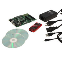
DV164136 Microchip Technology, DV164136 Datasheet - Page 87

DV164136
Manufacturer Part Number
DV164136
Description
DEVELOPMENT KIT FOR PIC18
Manufacturer
Microchip Technology
Series
PIC®r
Type
MCUr
Datasheets
1.DM183032.pdf
(38 pages)
2.DV164136.pdf
(448 pages)
3.DV164136.pdf
(6 pages)
4.DV164136.pdf
(446 pages)
5.DV164136.pdf
(4 pages)
6.DV164136.pdf
(18 pages)
Specifications of DV164136
Contents
Board, Cables, CDs, PICkit™ 3 Programmer, Power Supply
Processor To Be Evaluated
PIC18F8722, PIC18F87J11
Interface Type
RS-232, USB
Operating Supply Voltage
3.3 V, 5 V
Silicon Manufacturer
Microchip
Core Architecture
PIC
Core Sub-architecture
PIC18
Silicon Core Number
PIC18F
Silicon Family Name
PIC18F8xxx
Kit Contents
PIC18 Exp Brd PICkit 3 Cable CD PSU
Lead Free Status / RoHS Status
Lead free / RoHS Compliant
For Use With/related Products
PIC18F8722, PIC18F87J11
Lead Free Status / Rohs Status
Lead free / RoHS Compliant
Available stocks
Company
Part Number
Manufacturer
Quantity
Price
Company:
Part Number:
DV164136
Manufacturer:
MICROCHIP
Quantity:
12 000
- DM183032 PDF datasheet
- DV164136 PDF datasheet #2
- DV164136 PDF datasheet #3
- DV164136 PDF datasheet #4
- DV164136 PDF datasheet #5
- DV164136 PDF datasheet #6
- Current page: 87 of 446
- Download datasheet (7Mb)
5.5.3
The use of Indexed Literal Offset Addressing mode
effectively changes how the first 96 locations of Access
RAM (00h to 5Fh) are mapped. Rather than containing
just the contents of the bottom half of Bank 0, this mode
maps the contents from Bank 0 and a user defined
“window” that can be located anywhere in the data
memory space. The value of FSR2 establishes the
lower boundary of the addresses mapped into the
window, while the upper boundary is defined by FSR2
plus 95 (5Fh). Addresses in the Access RAM above
5Fh are mapped as previously described (see
Section 5.3.2 “Access Bank”). An example of Access
Bank remapping in this addressing mode is shown in
Figure 5-10.
FIGURE 5-10:
© 2008 Microchip Technology Inc.
Example Situation:
Locations in the region
from the FSR2 Pointer
(120h) to the pointer plus
05Fh (17Fh) are mapped
to
Access RAM (000h-05Fh).
Locations in Bank 0 from
060h to 07Fh are mapped,
as usual, to the middle half
of the Access Bank.
Special File Registers at
F80h through FFFh are
mapped to 80h through
FFh, as usual.
Bank 0 addresses below
5Fh can still be addressed
by using the BSR.
ADDWF
FSR2H:FSR2L = 120h
the
MAPPING THE ACCESS BANK IN
INDEXED LITERAL OFFSET MODE
f, d, a
bottom
of
REMAPPING THE ACCESS BANK WITH INDEXED LITERAL
OFFSET ADDRESSING
the
FFFh
05Fh
07Fh
17Fh
F00h
F80h
000h
100h
120h
200h
Data Memory
Window
Bank 14
Bank 15
through
Bank 1
Bank 0
Bank 1
Bank 2
Bank 0
SFRs
Remapping of the Access Bank applies only to opera-
tions using the Indexed Literal Offset mode. Operations
that use the BSR (Access RAM bit is ‘1’) will continue
to use Direct Addressing as before.
5.6
Enabling the extended instruction set adds eight
additional commands to the existing PIC18 instruction
set. These instructions are executed as described in
Section 26.2 “Extended Instruction Set”.
PIC18F8722 FAMILY
PIC18 Instruction Execution and
the Extended Instruction Set
Bank 1 “Window”
Access Bank
Bank 0
SFRs
DS39646C-page 85
00h
5Fh
7Fh
80h
FFh
Related parts for DV164136
Image
Part Number
Description
Manufacturer
Datasheet
Request
R

Part Number:
Description:
Manufacturer:
Microchip Technology Inc.
Datasheet:

Part Number:
Description:
Manufacturer:
Microchip Technology Inc.
Datasheet:

Part Number:
Description:
Manufacturer:
Microchip Technology Inc.
Datasheet:

Part Number:
Description:
Manufacturer:
Microchip Technology Inc.
Datasheet:

Part Number:
Description:
Manufacturer:
Microchip Technology Inc.
Datasheet:

Part Number:
Description:
Manufacturer:
Microchip Technology Inc.
Datasheet:

Part Number:
Description:
Manufacturer:
Microchip Technology Inc.
Datasheet:

Part Number:
Description:
Manufacturer:
Microchip Technology Inc.
Datasheet:


