C8051F360DK Silicon Laboratories Inc, C8051F360DK Datasheet - Page 145
C8051F360DK
Manufacturer Part Number
C8051F360DK
Description
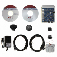
KIT DEV FOR C8051F360 FAMILY
Manufacturer
Silicon Laboratories Inc
Type
MCUr
Specifications of C8051F360DK
Contents
Evaluation Board, Power Supply, USB Cables, Adapter and Documentation
Processor To Be Evaluated
C8051F36x
Interface Type
USB
Lead Free Status / RoHS Status
Lead free / RoHS Compliant
For Use With/related Products
C8051F360, F361, F362, F363, F364, F365, F366, F367, F368, F369
Lead Free Status / Rohs Status
Lead free / RoHS Compliant
Other names
336-1410


C8051F360/1/2/3/4/5/6/7/8/9
14. Branch Target Cache
The C8051F36x device families incorporate a 32x4 byte branch target cache with a 4-byte prefetch
engine. Because the access time of the Flash memory is 40 ns, and the minimum instruction time is 10 ns
(C8051F360/1/2/3/4/5/6/7) or 20 ns (C8051F368/9), the branch target cache and prefetch engine are nec-
essary for full-speed code execution. Instructions are read from Flash memory four bytes at a time by the
prefetch engine, and given to the CIP-51 processor core to execute. When running linear code (code with-
out any jumps or branches), the prefetch engine alone allows instructions to be executed at full speed.
When a code branch occurs, a search is performed for the branch target (destination address) in the
cache. If the branch target information is found in the cache (called a “cache hit”), the instruction data is
read from the cache and immediately returned to the CIP-51 with no delay in code execution. If the branch
target is not found in the cache (called a “cache miss”), the processor may be stalled for up to four clock
cycles while the next set of four instructions is retrieved from Flash memory. Each time a cache miss
occurs, the requested instruction data is written to the cache if allowed by the current cache settings. A
data flow diagram of the interaction between the CIP-51 and the Branch Target Cache and Prefetch
Engine is shown in Figure 14.1.
Instruction
Data
CIP-51
Flash
Memory
Prefetch
Branch Target
Engine
Cache
Instruction Address
Figure 14.1. Branch Target Cache Data Flow
14.1. Cache and Prefetch Operation
The branch target cache maintains two sets of memory locations: “slots” and “tags”. A slot is where the
cached instruction data from Flash is stored. Each slot holds four consecutive code bytes. A tag contains
the 13 most significant bits of the corresponding Flash address for each four-byte slot. Thus, instruction
data is always cached along four-byte boundaries in code space. A tag also contains a “valid bit”, which
indicates whether a cache location contains valid instruction data. A special cache location (called the lin-
ear tag and slot), is reserved for use by the prefetch engine. The cache organization is shown in
Figure 14.2. Each time a Flash read is requested, the address is compared with all valid cache tag loca-
tions (including the linear tag). If any of the tag locations match the requested address, the data from that
slot is immediately provided to the CIP-51. If the requested address matches a location that is currently
being read by the prefetch engine, the CIP-51 will be stalled until the read is complete. If a match is not
found, the current prefetch operation is abandoned, and a new prefetch operation is initiated for the
requested instruction data. When the prefetch operation is finished, the CIP-51 begins executing the
instructions that were retrieved, and the prefetch engine begins reading the next four-byte word from Flash
memory. If the newly-fetched data also meets the criteria necessary to be cached, it will be written to the
cache in the slot indicated by the current replacement algorithm.
Rev. 1.0
145
Related parts for C8051F360DK
Image
Part Number
Description
Manufacturer
Datasheet
Request
R

Part Number:
Description:
SMD/C°/SINGLE-ENDED OUTPUT SILICON OSCILLATOR
Manufacturer:
Silicon Laboratories Inc
Part Number:
Description:
Manufacturer:
Silicon Laboratories Inc
Datasheet:
Part Number:
Description:
N/A N/A/SI4010 AES KEYFOB DEMO WITH LCD RX
Manufacturer:
Silicon Laboratories Inc
Datasheet:
Part Number:
Description:
N/A N/A/SI4010 SIMPLIFIED KEY FOB DEMO WITH LED RX
Manufacturer:
Silicon Laboratories Inc
Datasheet:
Part Number:
Description:
N/A/-40 TO 85 OC/EZLINK MODULE; F930/4432 HIGH BAND (REV E/B1)
Manufacturer:
Silicon Laboratories Inc
Part Number:
Description:
EZLink Module; F930/4432 Low Band (rev e/B1)
Manufacturer:
Silicon Laboratories Inc
Part Number:
Description:
I°/4460 10 DBM RADIO TEST CARD 434 MHZ
Manufacturer:
Silicon Laboratories Inc
Part Number:
Description:
I°/4461 14 DBM RADIO TEST CARD 868 MHZ
Manufacturer:
Silicon Laboratories Inc
Part Number:
Description:
I°/4463 20 DBM RFSWITCH RADIO TEST CARD 460 MHZ
Manufacturer:
Silicon Laboratories Inc
Part Number:
Description:
I°/4463 20 DBM RADIO TEST CARD 868 MHZ
Manufacturer:
Silicon Laboratories Inc
Part Number:
Description:
I°/4463 27 DBM RADIO TEST CARD 868 MHZ
Manufacturer:
Silicon Laboratories Inc
Part Number:
Description:
I°/4463 SKYWORKS 30 DBM RADIO TEST CARD 915 MHZ
Manufacturer:
Silicon Laboratories Inc
Part Number:
Description:
N/A N/A/-40 TO 85 OC/4463 RFMD 30 DBM RADIO TEST CARD 915 MHZ
Manufacturer:
Silicon Laboratories Inc
Part Number:
Description:
I°/4463 20 DBM RADIO TEST CARD 169 MHZ
Manufacturer:
Silicon Laboratories Inc