C8051F360DK Silicon Laboratories Inc, C8051F360DK Datasheet - Page 173
C8051F360DK
Manufacturer Part Number
C8051F360DK
Description
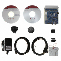
KIT DEV FOR C8051F360 FAMILY
Manufacturer
Silicon Laboratories Inc
Type
MCUr
Specifications of C8051F360DK
Contents
Evaluation Board, Power Supply, USB Cables, Adapter and Documentation
Processor To Be Evaluated
C8051F36x
Interface Type
USB
Lead Free Status / RoHS Status
Lead free / RoHS Compliant
For Use With/related Products
C8051F360, F361, F362, F363, F364, F365, F366, F367, F368, F369
Lead Free Status / Rohs Status
Lead free / RoHS Compliant
Other names
336-1410


C8051F360/1/2/3/4/5/6/7/8/9
16.3. External Oscillator Drive Circuit
The external oscillator circuit may drive an external crystal, ceramic resonator, capacitor, or RC network. A
CMOS clock may also provide a clock input. For a crystal or ceramic resonator configuration, the crystal/
resonator must be wired across the XTAL1 and XTAL2 pins as shown in Option 1 of Figure 16.1. A 10 MΩ
resistor also must be wired across the XTAL1 and XTAL2 pins for the crystal/resonator configuration. In
RC, capacitor, or CMOS clock configuration, the clock source should be wired to the XTAL2 pin as shown
in Option 2, 3, or 4 of Figure 16.1. The type of external oscillator must be selected in the OSCXCN register,
and the frequency control bits (XFCN) must be selected appropriately (see SFR Definition 16.5).
Important Note on External Oscillator Usage: Port pins must be configured when using the external
oscillator circuit. When the external oscillator drive circuit is enabled in crystal/resonator mode, Port pins
P0.5 and P0.6 (C8051F360/3) or P0.2 and P0.3 (C8051F361/2/4/5/6/7/8/9) are used as XTAL1 and XTAL2
respectively. When the external oscillator drive circuit is enabled in capacitor, RC, or CMOS clock mode,
Port pin P0.6 (C8051F360/3) or P0.3 (C8051F361/2/4/5/6/7/8/9) is used as XTAL2. The Port I/O Crossbar
should be configured to skip the Port pins used by the oscillator circuit; see Section “17.1. Priority Crossbar
Decoder” on page 185 for Crossbar configuration. Additionally, when using the external oscillator circuit in
crystal/resonator, capacitor, or RC mode, the associated Port pins should be configured as analog inputs.
In CMOS clock mode, the associated pin should be configured as a digital input. See Section “17.2. Port
I/O Initialization” on page 187 for details on Port input mode selection.
16.4. System Clock Selection
The internal oscillator requires little start-up time, and may be enabled and selected as the system clock in
the same write to OSCICN. External crystals and ceramic resonators typically require a start-up time
before they are settled and ready for use as the system clock. The Crystal Valid Flag (XTLVLD in register
OSCXCN) is set to ‘1’ by hardware when the external oscillator is settled. To avoid reading a false
XTLVLD, in crystal mode software should delay at least 1 ms between enabling the external oscillator and
checking XTLVLD. RC and C modes typically require no startup time. The PLL also requires time to lock
onto the desired frequency, and the PLL Lock Flag (PLLLCK in register PLL0CN) is set to ‘1’ by hardware
once the PLL is locked on the correct frequency.
The CLKSL1-0 bits in register CLKSEL select which oscillator source generates the system clock.
CLKSL1-0 must be set to ‘01’ for the system clock to run from the external oscillator; however the external
oscillator may still clock certain peripherals, such as the timers and PCA, when the internal oscillator or the
PLL is selected as the system clock. The system clock may be switched on-the-fly between the internal
and external oscillators or the PLL, so long as the selected oscillator source is enabled and settled.
Rev. 1.0
173
Related parts for C8051F360DK
Image
Part Number
Description
Manufacturer
Datasheet
Request
R

Part Number:
Description:
SMD/C°/SINGLE-ENDED OUTPUT SILICON OSCILLATOR
Manufacturer:
Silicon Laboratories Inc
Part Number:
Description:
Manufacturer:
Silicon Laboratories Inc
Datasheet:
Part Number:
Description:
N/A N/A/SI4010 AES KEYFOB DEMO WITH LCD RX
Manufacturer:
Silicon Laboratories Inc
Datasheet:
Part Number:
Description:
N/A N/A/SI4010 SIMPLIFIED KEY FOB DEMO WITH LED RX
Manufacturer:
Silicon Laboratories Inc
Datasheet:
Part Number:
Description:
N/A/-40 TO 85 OC/EZLINK MODULE; F930/4432 HIGH BAND (REV E/B1)
Manufacturer:
Silicon Laboratories Inc
Part Number:
Description:
EZLink Module; F930/4432 Low Band (rev e/B1)
Manufacturer:
Silicon Laboratories Inc
Part Number:
Description:
I°/4460 10 DBM RADIO TEST CARD 434 MHZ
Manufacturer:
Silicon Laboratories Inc
Part Number:
Description:
I°/4461 14 DBM RADIO TEST CARD 868 MHZ
Manufacturer:
Silicon Laboratories Inc
Part Number:
Description:
I°/4463 20 DBM RFSWITCH RADIO TEST CARD 460 MHZ
Manufacturer:
Silicon Laboratories Inc
Part Number:
Description:
I°/4463 20 DBM RADIO TEST CARD 868 MHZ
Manufacturer:
Silicon Laboratories Inc
Part Number:
Description:
I°/4463 27 DBM RADIO TEST CARD 868 MHZ
Manufacturer:
Silicon Laboratories Inc
Part Number:
Description:
I°/4463 SKYWORKS 30 DBM RADIO TEST CARD 915 MHZ
Manufacturer:
Silicon Laboratories Inc
Part Number:
Description:
N/A N/A/-40 TO 85 OC/4463 RFMD 30 DBM RADIO TEST CARD 915 MHZ
Manufacturer:
Silicon Laboratories Inc
Part Number:
Description:
I°/4463 20 DBM RADIO TEST CARD 169 MHZ
Manufacturer:
Silicon Laboratories Inc