C8051F360DK Silicon Laboratories Inc, C8051F360DK Datasheet - Page 157
C8051F360DK
Manufacturer Part Number
C8051F360DK
Description
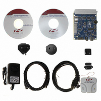
KIT DEV FOR C8051F360 FAMILY
Manufacturer
Silicon Laboratories Inc
Type
MCUr
Specifications of C8051F360DK
Contents
Evaluation Board, Power Supply, USB Cables, Adapter and Documentation
Processor To Be Evaluated
C8051F36x
Interface Type
USB
Lead Free Status / RoHS Status
Lead free / RoHS Compliant
For Use With/related Products
C8051F360, F361, F362, F363, F364, F365, F366, F367, F368, F369
Lead Free Status / Rohs Status
Lead free / RoHS Compliant
Other names
336-1410


15.4. Multiplexed and Non-multiplexed Selection
The External Memory Interface is capable of acting in a Multiplexed mode or a Non-multiplexed mode,
depending on the state of the EMD2 (EMI0CF.4) bit.
15.4.1. Multiplexed Configuration
In Multiplexed mode, the Data Bus and the lower 8-bits of the Address Bus share the same Port pins:
AD[7:0]. In this mode, an external latch (74HC373 or equivalent logic gate) is used to hold the lower 8-bits
of the RAM address. The external latch is controlled by the ALE (Address Latch Enable) signal, which is
driven by the External Memory Interface logic. An example of a Multiplexed Configuration is shown in
Figure 15.1.
In Multiplexed mode, the external MOVX operation can be broken into two phases delineated by the state
of the ALE signal. During the first phase, ALE is high and the lower 8-bits of the Address Bus are pre-
sented to AD[7:0]. During this phase, the address latch is configured such that the ‘Q’ outputs reflect the
states of the ‘D’ inputs. When ALE falls, signaling the beginning of the second phase, the address latch
outputs remain fixed and are no longer dependent on the latch inputs. Later in the second phase, the Data
Bus controls the state of the AD[7:0] port at the time /RD or /WR is asserted.
See Section “15.6.2. Multiplexed Mode” on page 165 for more information.
E
M
I
F
AD[7:0]
A[15:8]
/WR
ALE
/RD
Figure 15.1. Multiplexed Configuration Example
ADDRESS/DATA BUS
ADDRESS BUS
C8051F360/1/2/3/4/5/6/7/8/9
Rev. 1.0
V
DD
8
(Optional)
74HC373
G
D
Q
A[15:8]
A[7:0]
I/O[7:0]
CE
WE
OE
64 K X 8
SRAM
157
Related parts for C8051F360DK
Image
Part Number
Description
Manufacturer
Datasheet
Request
R

Part Number:
Description:
SMD/C°/SINGLE-ENDED OUTPUT SILICON OSCILLATOR
Manufacturer:
Silicon Laboratories Inc
Part Number:
Description:
Manufacturer:
Silicon Laboratories Inc
Datasheet:
Part Number:
Description:
N/A N/A/SI4010 AES KEYFOB DEMO WITH LCD RX
Manufacturer:
Silicon Laboratories Inc
Datasheet:
Part Number:
Description:
N/A N/A/SI4010 SIMPLIFIED KEY FOB DEMO WITH LED RX
Manufacturer:
Silicon Laboratories Inc
Datasheet:
Part Number:
Description:
N/A/-40 TO 85 OC/EZLINK MODULE; F930/4432 HIGH BAND (REV E/B1)
Manufacturer:
Silicon Laboratories Inc
Part Number:
Description:
EZLink Module; F930/4432 Low Band (rev e/B1)
Manufacturer:
Silicon Laboratories Inc
Part Number:
Description:
I°/4460 10 DBM RADIO TEST CARD 434 MHZ
Manufacturer:
Silicon Laboratories Inc
Part Number:
Description:
I°/4461 14 DBM RADIO TEST CARD 868 MHZ
Manufacturer:
Silicon Laboratories Inc
Part Number:
Description:
I°/4463 20 DBM RFSWITCH RADIO TEST CARD 460 MHZ
Manufacturer:
Silicon Laboratories Inc
Part Number:
Description:
I°/4463 20 DBM RADIO TEST CARD 868 MHZ
Manufacturer:
Silicon Laboratories Inc
Part Number:
Description:
I°/4463 27 DBM RADIO TEST CARD 868 MHZ
Manufacturer:
Silicon Laboratories Inc
Part Number:
Description:
I°/4463 SKYWORKS 30 DBM RADIO TEST CARD 915 MHZ
Manufacturer:
Silicon Laboratories Inc
Part Number:
Description:
N/A N/A/-40 TO 85 OC/4463 RFMD 30 DBM RADIO TEST CARD 915 MHZ
Manufacturer:
Silicon Laboratories Inc
Part Number:
Description:
I°/4463 20 DBM RADIO TEST CARD 169 MHZ
Manufacturer:
Silicon Laboratories Inc