C8051F360DK Silicon Laboratories Inc, C8051F360DK Datasheet - Page 24
C8051F360DK
Manufacturer Part Number
C8051F360DK
Description
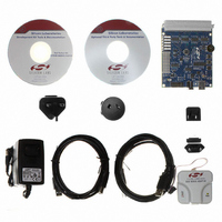
KIT DEV FOR C8051F360 FAMILY
Manufacturer
Silicon Laboratories Inc
Type
MCUr
Specifications of C8051F360DK
Contents
Evaluation Board, Power Supply, USB Cables, Adapter and Documentation
Processor To Be Evaluated
C8051F36x
Interface Type
USB
Lead Free Status / RoHS Status
Lead free / RoHS Compliant
For Use With/related Products
C8051F360, F361, F362, F363, F364, F365, F366, F367, F368, F369
Lead Free Status / Rohs Status
Lead free / RoHS Compliant
Other names
336-1410


C8051F360/1/2/3/4/5/6/7/8/9
1.2.
The CIP-51 has a standard 8051 program and data address configuration. It includes 256 bytes of data
RAM, with the upper 128 bytes dual-mapped. Indirect addressing accesses the upper 128 bytes of general
purpose RAM, and direct addressing accesses the 128 byte SFR address space. The lower 128 bytes of
RAM are accessible via direct and indirect addressing. The first 32 bytes are addressable as four banks of
general purpose registers, and the next 16 bytes can be byte addressable or bit addressable.
Program memory consists of 32/16 kB of Flash. This memory may be reprogrammed in-system in 1024
byte sectors, and requires no special off-chip programming voltage. See Figure 1.6 for the MCU system
memory map.
1.3.
The C8051F36x devices include on-chip Silicon Labs 2-Wire (C2) debug circuitry that provides non-intru-
sive, full speed, in-circuit debugging of the production part installed in the end application.
Silicon Labs' debugging system supports inspection and modification of memory and registers, break-
points, and single stepping. No additional target RAM, program memory, timers, or communications chan-
24
0x7BFF
0x7C00
0x3FFF
0x0000
0x4000
0x0000
On-Chip Memory
On-Chip Debug Circuitry
PROGRAM MEMORY
C8051F360/1/2/3/4/5/6/7
Programmable in 1024
Programmable in 1024
Byte Sectors)
C8051F368/9
Byte Sectors)
RESERVED
RESERVED
(In-System
(In-System
FLASH
FLASH
Figure 1.6. On-Board Memory Map
0xFFFF
0x03FF
0x0400
0x0000
Rev. 1.0
0xFF
0x7F
0x2F
0x1F
0x80
0x30
0x20
0x00
XRAM - 1024 Bytes
0x0000 to 0x03FF, wrapped
(accessable using MOVX
Same 1024 bytes as from
on 1024-byte boundaries
(Indirect Addressing
(Direct and Indirect
General Purpose
Upper 128 RAM
Bit Addressable
Addressing)
INTERNAL DATA ADDRESS SPACE
EXTERNAL DATA ADDRESS SPACE
instruction)
Registers
Only)
DATA MEMORY
(Direct Addressing Only)
Special Function
Lower 128 RAM
(Direct and Indirect
Addressing)
Register's
Related parts for C8051F360DK
Image
Part Number
Description
Manufacturer
Datasheet
Request
R

Part Number:
Description:
SMD/C°/SINGLE-ENDED OUTPUT SILICON OSCILLATOR
Manufacturer:
Silicon Laboratories Inc
Part Number:
Description:
Manufacturer:
Silicon Laboratories Inc
Datasheet:
Part Number:
Description:
N/A N/A/SI4010 AES KEYFOB DEMO WITH LCD RX
Manufacturer:
Silicon Laboratories Inc
Datasheet:
Part Number:
Description:
N/A N/A/SI4010 SIMPLIFIED KEY FOB DEMO WITH LED RX
Manufacturer:
Silicon Laboratories Inc
Datasheet:
Part Number:
Description:
N/A/-40 TO 85 OC/EZLINK MODULE; F930/4432 HIGH BAND (REV E/B1)
Manufacturer:
Silicon Laboratories Inc
Part Number:
Description:
EZLink Module; F930/4432 Low Band (rev e/B1)
Manufacturer:
Silicon Laboratories Inc
Part Number:
Description:
I°/4460 10 DBM RADIO TEST CARD 434 MHZ
Manufacturer:
Silicon Laboratories Inc
Part Number:
Description:
I°/4461 14 DBM RADIO TEST CARD 868 MHZ
Manufacturer:
Silicon Laboratories Inc
Part Number:
Description:
I°/4463 20 DBM RFSWITCH RADIO TEST CARD 460 MHZ
Manufacturer:
Silicon Laboratories Inc
Part Number:
Description:
I°/4463 20 DBM RADIO TEST CARD 868 MHZ
Manufacturer:
Silicon Laboratories Inc
Part Number:
Description:
I°/4463 27 DBM RADIO TEST CARD 868 MHZ
Manufacturer:
Silicon Laboratories Inc
Part Number:
Description:
I°/4463 SKYWORKS 30 DBM RADIO TEST CARD 915 MHZ
Manufacturer:
Silicon Laboratories Inc
Part Number:
Description:
N/A N/A/-40 TO 85 OC/4463 RFMD 30 DBM RADIO TEST CARD 915 MHZ
Manufacturer:
Silicon Laboratories Inc
Part Number:
Description:
I°/4463 20 DBM RADIO TEST CARD 169 MHZ
Manufacturer:
Silicon Laboratories Inc