C8051F360DK Silicon Laboratories Inc, C8051F360DK Datasheet - Page 25
C8051F360DK
Manufacturer Part Number
C8051F360DK
Description
KIT DEV FOR C8051F360 FAMILY
Manufacturer
Silicon Laboratories Inc
Type
MCUr
Specifications of C8051F360DK
Contents
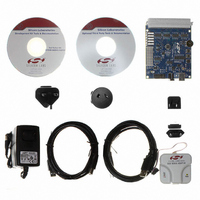
Evaluation Board, Power Supply, USB Cables, Adapter and Documentation
Processor To Be Evaluated
C8051F36x
Interface Type
USB
Lead Free Status / RoHS Status
Lead free / RoHS Compliant
For Use With/related Products
C8051F360, F361, F362, F363, F364, F365, F366, F367, F368, F369
Lead Free Status / Rohs Status
Lead free / RoHS Compliant
Other names
336-1410


nels are required. All the digital and analog peripherals are functional and work correctly while debugging.
All the peripherals (except for the ADC and SMBus) are stalled when the MCU is halted, during single
stepping, or at a breakpoint in order to keep them synchronized.
The C8051F360DK development kit provides all the hardware and software necessary to develop applica-
tion code and perform in-circuit debugging with the C8051F36x MCUs. The kit includes software with a
developer's studio and debugger, an integrated 8051 assembler, and a debug adapter. It also has a target
application board with the associated MCU installed and prototyping area, plus the required cables, and
wall-mount power supply. The Development Kit requires a PC running Windows98SE or later.
The Silicon Labs IDE interface is a vastly superior developing and debugging configuration, compared to
standard MCU emulators that use on-board "ICE Chips" and require the MCU in the application board to
be socketed. Silicon Labs' debug paradigm increases ease of use and preserves the performance of the
precision analog peripherals.
1.4.
C8051F36x devices include up to 39 I/O pins (four byte-wide Ports and one 7-bit-wide Port). The
C8051F36x Ports behave like typical 8051 Ports with a few enhancements. Each Port pin may be config-
ured as an analog input or a digital I/O pin. Pins selected as digital I/Os may additionally be configured for
push-pull or open-drain output. The “weak pullups” that are fixed on typical 8051 devices may be globally
disabled, providing power savings capabilities.
Programmable Digital I/O and Crossbar
WINDOWS 2000 or later
Figure 1.7. Development/In-System Debug Diagram
C2 (x2), VDD, GND
VDD
Development Environment
GND
Silicon Labs Integrated
C8051F360
C8051F360/1/2/3/4/5/6/7/8/9
Rev. 1.0
Adapter
TARGET PCB
Debug
25
Related parts for C8051F360DK
Image
Part Number
Description
Manufacturer
Datasheet
Request
R

Part Number:
Description:
SMD/C°/SINGLE-ENDED OUTPUT SILICON OSCILLATOR
Manufacturer:
Silicon Laboratories Inc
Part Number:
Description:
Manufacturer:
Silicon Laboratories Inc
Datasheet:
Part Number:
Description:
N/A N/A/SI4010 AES KEYFOB DEMO WITH LCD RX
Manufacturer:
Silicon Laboratories Inc
Datasheet:
Part Number:
Description:
N/A N/A/SI4010 SIMPLIFIED KEY FOB DEMO WITH LED RX
Manufacturer:
Silicon Laboratories Inc
Datasheet:
Part Number:
Description:
N/A/-40 TO 85 OC/EZLINK MODULE; F930/4432 HIGH BAND (REV E/B1)
Manufacturer:
Silicon Laboratories Inc
Part Number:
Description:
EZLink Module; F930/4432 Low Band (rev e/B1)
Manufacturer:
Silicon Laboratories Inc
Part Number:
Description:
I°/4460 10 DBM RADIO TEST CARD 434 MHZ
Manufacturer:
Silicon Laboratories Inc
Part Number:
Description:
I°/4461 14 DBM RADIO TEST CARD 868 MHZ
Manufacturer:
Silicon Laboratories Inc
Part Number:
Description:
I°/4463 20 DBM RFSWITCH RADIO TEST CARD 460 MHZ
Manufacturer:
Silicon Laboratories Inc
Part Number:
Description:
I°/4463 20 DBM RADIO TEST CARD 868 MHZ
Manufacturer:
Silicon Laboratories Inc
Part Number:
Description:
I°/4463 27 DBM RADIO TEST CARD 868 MHZ
Manufacturer:
Silicon Laboratories Inc
Part Number:
Description:
I°/4463 SKYWORKS 30 DBM RADIO TEST CARD 915 MHZ
Manufacturer:
Silicon Laboratories Inc
Part Number:
Description:
N/A N/A/-40 TO 85 OC/4463 RFMD 30 DBM RADIO TEST CARD 915 MHZ
Manufacturer:
Silicon Laboratories Inc
Part Number:
Description:
I°/4463 20 DBM RADIO TEST CARD 169 MHZ
Manufacturer:
Silicon Laboratories Inc