C8051F360DK Silicon Laboratories Inc, C8051F360DK Datasheet - Page 27
C8051F360DK
Manufacturer Part Number
C8051F360DK
Description
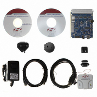
KIT DEV FOR C8051F360 FAMILY
Manufacturer
Silicon Laboratories Inc
Type
MCUr
Specifications of C8051F360DK
Contents
Evaluation Board, Power Supply, USB Cables, Adapter and Documentation
Processor To Be Evaluated
C8051F36x
Interface Type
USB
Lead Free Status / RoHS Status
Lead free / RoHS Compliant
For Use With/related Products
C8051F360, F361, F362, F363, F364, F365, F366, F367, F368, F369
Lead Free Status / Rohs Status
Lead free / RoHS Compliant
Other names
336-1410


real-time clock functionality, where the PCA is clocked by an external source while the internal oscillator
drives the system clock.
Each capture/compare module can be configured to operate in one of six modes: Edge-Triggered Capture,
Software Timer, High Speed Output, 8- or 16-bit Pulse Width Modulator, or Frequency Output. Additionally,
Capture/Compare Module 5 offers watchdog timer (WDT) capabilities. Following a system reset, Module 5
is configured and enabled in WDT mode. The PCA Capture/Compare Module I/O and External Clock Input
may be routed to Port I/O via the Digital Crossbar.
1.7.
The C8051F360/1/2/6/7/8/9 devices include an on-chip 10-bit SAR ADC with up to 21 channels for the dif-
ferential input multiplexer. With a maximum throughput of 200 ksps, the ADC offers true 10-bit linearity with
an INL and DNL of ±1 LSB. The ADC system includes a configurable analog multiplexer that selects both
positive and negative ADC inputs. Ports1-3 are available as an ADC inputs; additionally, the on-chip Tem-
perature Sensor output and the power supply voltage (V
may shut down the ADC to save power.
Conversions can be started in six ways: a software command, an overflow of Timer 0, 1, 2, or 3, or an
external convert start signal (CNVSTR). This flexibility allows the start of conversion to be triggered by soft-
ware events, a periodic signal (timer overflows), or external HW signals. Conversion completions are indi-
10-Bit Analog to Digital Converter
Capture/Compare
Module 0
SYSCLK/12
SYSCLK/4
Timer 0 Overflow
SYSCLK
External Clock/8
ECI
Capture/Compare
Module 1
CLOCK
MUX
PCA
Figure 1.10. PCA Block Diagram
16-Bit Counter/Timer
Capture/Compare
Module 2
Crossbar
Port I/O
C8051F360/1/2/3/4/5/6/7/8/9
Rev. 1.0
DD
Capture/Compare
) are available as ADC inputs. User firmware
Module 3
Capture/Compare
Module 4
Capture/Compare
Module 5
27
Related parts for C8051F360DK
Image
Part Number
Description
Manufacturer
Datasheet
Request
R

Part Number:
Description:
SMD/C°/SINGLE-ENDED OUTPUT SILICON OSCILLATOR
Manufacturer:
Silicon Laboratories Inc
Part Number:
Description:
Manufacturer:
Silicon Laboratories Inc
Datasheet:
Part Number:
Description:
N/A N/A/SI4010 AES KEYFOB DEMO WITH LCD RX
Manufacturer:
Silicon Laboratories Inc
Datasheet:
Part Number:
Description:
N/A N/A/SI4010 SIMPLIFIED KEY FOB DEMO WITH LED RX
Manufacturer:
Silicon Laboratories Inc
Datasheet:
Part Number:
Description:
N/A/-40 TO 85 OC/EZLINK MODULE; F930/4432 HIGH BAND (REV E/B1)
Manufacturer:
Silicon Laboratories Inc
Part Number:
Description:
EZLink Module; F930/4432 Low Band (rev e/B1)
Manufacturer:
Silicon Laboratories Inc
Part Number:
Description:
I°/4460 10 DBM RADIO TEST CARD 434 MHZ
Manufacturer:
Silicon Laboratories Inc
Part Number:
Description:
I°/4461 14 DBM RADIO TEST CARD 868 MHZ
Manufacturer:
Silicon Laboratories Inc
Part Number:
Description:
I°/4463 20 DBM RFSWITCH RADIO TEST CARD 460 MHZ
Manufacturer:
Silicon Laboratories Inc
Part Number:
Description:
I°/4463 20 DBM RADIO TEST CARD 868 MHZ
Manufacturer:
Silicon Laboratories Inc
Part Number:
Description:
I°/4463 27 DBM RADIO TEST CARD 868 MHZ
Manufacturer:
Silicon Laboratories Inc
Part Number:
Description:
I°/4463 SKYWORKS 30 DBM RADIO TEST CARD 915 MHZ
Manufacturer:
Silicon Laboratories Inc
Part Number:
Description:
N/A N/A/-40 TO 85 OC/4463 RFMD 30 DBM RADIO TEST CARD 915 MHZ
Manufacturer:
Silicon Laboratories Inc
Part Number:
Description:
I°/4463 20 DBM RADIO TEST CARD 169 MHZ
Manufacturer:
Silicon Laboratories Inc