C8051F360DK Silicon Laboratories Inc, C8051F360DK Datasheet - Page 28
C8051F360DK
Manufacturer Part Number
C8051F360DK
Description
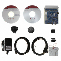
KIT DEV FOR C8051F360 FAMILY
Manufacturer
Silicon Laboratories Inc
Type
MCUr
Specifications of C8051F360DK
Contents
Evaluation Board, Power Supply, USB Cables, Adapter and Documentation
Processor To Be Evaluated
C8051F36x
Interface Type
USB
Lead Free Status / RoHS Status
Lead free / RoHS Compliant
For Use With/related Products
C8051F360, F361, F362, F363, F364, F365, F366, F367, F368, F369
Lead Free Status / Rohs Status
Lead free / RoHS Compliant
Other names
336-1410


C8051F360/1/2/3/4/5/6/7/8/9
cated by a status bit and an interrupt (if enabled). The resulting 10-bit data word is latched into the ADC
data SFRs upon completion of a conversion.
Window compare registers for the ADC data can be configured to interrupt the controller when ADC data is
either within or outside of a specified range. The ADC can monitor a key voltage continuously in back-
ground mode, but not interrupt the controller unless the converted data is within/outside the specified
range.
1.8.
C8051F36x devices include two on-chip voltage comparators that are enabled/disabled and configured via
user software. Port I/O pins may be configured as comparator inputs via a selection mux. Two comparator
outputs may be routed to a Port pin if desired: a latched output and/or an unlatched (asynchronous) output.
Comparator response time is programmable, allowing the user to select between high-speed and low-
power modes. Positive and negative hysteresis are also configurable.
Comparator interrupts may be generated on rising, falling, or both edges. When in IDLE mode, these inter-
rupts may be used as a “wake-up” source. Comparator0 may also be configured as a reset source.
Figure 1.12 shows the Comparator0 block diagram, and Figure 1.13 shows the Comparator1 block dia-
gram.
Note: The first Port I/O pins shown in Figure 1.12 and Figure 1.13 are for the 48-pin (C8051F360/3)
devices. The second set of Port I/O pins are for the 32-pin and 28-pin (C8051F361/2/4/5/6/7/8/9) devices.
Please refer to the CPTnMX registers (SFR Definition 8.2 and SFR Definition 8.5) for more information.
28
P3.1-3.4 available on
P3.1-3.4 available on
P1.0-1.3 available on
C8051F361/2/6/7/8/9
P1.0-1.3 available on
C8051F361/2/6/7/8/9
C8051F360/1/6/8
C8051F360/1/6/8
Comparators
Sensor
Temp
VREF
GND
VDD
P1.0
P1.7
P2.0
P2.7
P3.0
P3.4
P1.0
P1.7
P2.0
P2.7
P3.0
P3.4
Figure 1.11. 10-Bit ADC Block Diagram
23-to-1
23-to-1
AMUX
AMUX
AMX0P
AMX0N
Rev. 1.0
(+)
(-)
ADC0CF
ADC
10-Bit
VDD
SAR
ADC0GTH ADC0GTL
ADC0LTH
ADC0CN
ADC0LTL
Conversion
Start
100
000
001
010
011
101
32
AD0WINT
Compare
Window
AD0BUSY (W)
Timer 0 Overflow
Timer 2 Overflow
Timer 1 Overflow
CNVSTR Input
Timer 3 Overflow
Logic
Related parts for C8051F360DK
Image
Part Number
Description
Manufacturer
Datasheet
Request
R

Part Number:
Description:
SMD/C°/SINGLE-ENDED OUTPUT SILICON OSCILLATOR
Manufacturer:
Silicon Laboratories Inc
Part Number:
Description:
Manufacturer:
Silicon Laboratories Inc
Datasheet:
Part Number:
Description:
N/A N/A/SI4010 AES KEYFOB DEMO WITH LCD RX
Manufacturer:
Silicon Laboratories Inc
Datasheet:
Part Number:
Description:
N/A N/A/SI4010 SIMPLIFIED KEY FOB DEMO WITH LED RX
Manufacturer:
Silicon Laboratories Inc
Datasheet:
Part Number:
Description:
N/A/-40 TO 85 OC/EZLINK MODULE; F930/4432 HIGH BAND (REV E/B1)
Manufacturer:
Silicon Laboratories Inc
Part Number:
Description:
EZLink Module; F930/4432 Low Band (rev e/B1)
Manufacturer:
Silicon Laboratories Inc
Part Number:
Description:
I°/4460 10 DBM RADIO TEST CARD 434 MHZ
Manufacturer:
Silicon Laboratories Inc
Part Number:
Description:
I°/4461 14 DBM RADIO TEST CARD 868 MHZ
Manufacturer:
Silicon Laboratories Inc
Part Number:
Description:
I°/4463 20 DBM RFSWITCH RADIO TEST CARD 460 MHZ
Manufacturer:
Silicon Laboratories Inc
Part Number:
Description:
I°/4463 20 DBM RADIO TEST CARD 868 MHZ
Manufacturer:
Silicon Laboratories Inc
Part Number:
Description:
I°/4463 27 DBM RADIO TEST CARD 868 MHZ
Manufacturer:
Silicon Laboratories Inc
Part Number:
Description:
I°/4463 SKYWORKS 30 DBM RADIO TEST CARD 915 MHZ
Manufacturer:
Silicon Laboratories Inc
Part Number:
Description:
N/A N/A/-40 TO 85 OC/4463 RFMD 30 DBM RADIO TEST CARD 915 MHZ
Manufacturer:
Silicon Laboratories Inc
Part Number:
Description:
I°/4463 20 DBM RADIO TEST CARD 169 MHZ
Manufacturer:
Silicon Laboratories Inc