C8051F360DK Silicon Laboratories Inc, C8051F360DK Datasheet - Page 70
C8051F360DK
Manufacturer Part Number
C8051F360DK
Description
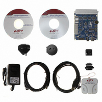
KIT DEV FOR C8051F360 FAMILY
Manufacturer
Silicon Laboratories Inc
Type
MCUr
Specifications of C8051F360DK
Contents
Evaluation Board, Power Supply, USB Cables, Adapter and Documentation
Processor To Be Evaluated
C8051F36x
Interface Type
USB
Lead Free Status / RoHS Status
Lead free / RoHS Compliant
For Use With/related Products
C8051F360, F361, F362, F363, F364, F365, F366, F367, F368, F369
Lead Free Status / Rohs Status
Lead free / RoHS Compliant
Other names
336-1410


C8051F360/1/2/3/4/5/6/7/8/9
8.
C8051F36x devices include two on-chip programmable voltage comparators, Comparator0 and
Comparator1, shown in Figure 8.1 and Figure 8.2 (Note: the port pin Comparator inputs differ between
C8051F36x devices. The first Port I/O pin shown is for C8051F360/3 devices).
The comparators offer programmable response time and hysteresis, an analog input multiplexer, and two
outputs that are optionally available at the Port pins: a synchronous “latched” output (CP0 and CP1), or an
asynchronous “raw” output (CP0A and CP1A). The asynchronous CP0A and CP1A signals are available
even when the system clock is not active. This allows the Comparators to operate and generate an output
with the device in STOP mode. When assigned to a Port pin, the Comparator outputs may be configured
as open drain or push-pull (see Section “17.2. Port I/O Initialization” on page 187). Comparator0 may also
be used as a reset source (see Section “12.5. Comparator0 Reset” on page 131).
The Comparator inputs are selected in the CPT0MX and CPT1MX registers (SFR Definition 8.2 and SFR
Definition 8.5). The CMXnP1–CMXnP0 bits select the Comparator positive input; the CMXnN1–CMXnN0
bits select the Comparator negative input.
Important Note About Comparator Inputs: The Port pins selected as comparator inputs should be con-
figured as analog inputs in their associated Port configuration register, and configured to be skipped by the
Crossbar (for details on Port configuration, see Section “17.3. General Purpose Port I/O” on page 190).
70
Comparators
CMX0N3
CMX0N2
CMX0N1
CMX0N0
CMX0P1
CMX0P0
Figure 8.1. Comparator0 Functional Block Diagram
P1.4 / P1.0
P2.3 / P1.4
P3.1 / P2.0
P3.5 / P2.4
P1.5 / P1.1
P2.4 / P1.5
P3.2 / P2.1
P3.6 / P2.5
CP0HYP1
CP0HYP0
CP0HYN1
CP0HYN0
CP0OUT
CP0RIF
CP0EN
CP0FIF
CP0 +
CP0 -
CP0MD1
CP0MD0
CP0RIE
CP0FIE
Rev. 1.0
+
-
VDD
GND
CP0RIF
CP0FIF
Decision
Reset
Tree
(SYNCHRONIZER)
D
SET
CLR
Q
Q
0
1
0
1
D
SET
CLR
Q
Q
CP0EN
Crossbar
0
1
EA
0
1
CP0A
Interrupt
CP0
CP0
Related parts for C8051F360DK
Image
Part Number
Description
Manufacturer
Datasheet
Request
R

Part Number:
Description:
SMD/C°/SINGLE-ENDED OUTPUT SILICON OSCILLATOR
Manufacturer:
Silicon Laboratories Inc
Part Number:
Description:
Manufacturer:
Silicon Laboratories Inc
Datasheet:
Part Number:
Description:
N/A N/A/SI4010 AES KEYFOB DEMO WITH LCD RX
Manufacturer:
Silicon Laboratories Inc
Datasheet:
Part Number:
Description:
N/A N/A/SI4010 SIMPLIFIED KEY FOB DEMO WITH LED RX
Manufacturer:
Silicon Laboratories Inc
Datasheet:
Part Number:
Description:
N/A/-40 TO 85 OC/EZLINK MODULE; F930/4432 HIGH BAND (REV E/B1)
Manufacturer:
Silicon Laboratories Inc
Part Number:
Description:
EZLink Module; F930/4432 Low Band (rev e/B1)
Manufacturer:
Silicon Laboratories Inc
Part Number:
Description:
I°/4460 10 DBM RADIO TEST CARD 434 MHZ
Manufacturer:
Silicon Laboratories Inc
Part Number:
Description:
I°/4461 14 DBM RADIO TEST CARD 868 MHZ
Manufacturer:
Silicon Laboratories Inc
Part Number:
Description:
I°/4463 20 DBM RFSWITCH RADIO TEST CARD 460 MHZ
Manufacturer:
Silicon Laboratories Inc
Part Number:
Description:
I°/4463 20 DBM RADIO TEST CARD 868 MHZ
Manufacturer:
Silicon Laboratories Inc
Part Number:
Description:
I°/4463 27 DBM RADIO TEST CARD 868 MHZ
Manufacturer:
Silicon Laboratories Inc
Part Number:
Description:
I°/4463 SKYWORKS 30 DBM RADIO TEST CARD 915 MHZ
Manufacturer:
Silicon Laboratories Inc
Part Number:
Description:
N/A N/A/-40 TO 85 OC/4463 RFMD 30 DBM RADIO TEST CARD 915 MHZ
Manufacturer:
Silicon Laboratories Inc
Part Number:
Description:
I°/4463 20 DBM RADIO TEST CARD 169 MHZ
Manufacturer:
Silicon Laboratories Inc