C8051F360DK Silicon Laboratories Inc, C8051F360DK Datasheet - Page 151
C8051F360DK
Manufacturer Part Number
C8051F360DK
Description
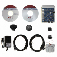
KIT DEV FOR C8051F360 FAMILY
Manufacturer
Silicon Laboratories Inc
Type
MCUr
Specifications of C8051F360DK
Contents
Evaluation Board, Power Supply, USB Cables, Adapter and Documentation
Processor To Be Evaluated
C8051F36x
Interface Type
USB
Lead Free Status / RoHS Status
Lead free / RoHS Compliant
For Use With/related Products
C8051F360, F361, F362, F363, F364, F365, F366, F367, F368, F369
Lead Free Status / Rohs Status
Lead free / RoHS Compliant
Other names
336-1410


Bit 7:
Bit 6:
Bit 5:
Bits 4–0: CHSLOT: Cache Slot Pointer.
SFR Page:
SFR Address:
CHPUSH
R/W
Bit7
CHPUSH: Cache Push Enable.
This bit enables cache push operations, which will lock information in cache slots using
MOVC instructions.
0: Cache push operations are disabled.
1: Cache push operations are enabled. When a MOVC read is executed, the requested 4-
Note:No more than 30 cache slots should be locked at one time, since the entire cache will be unlocked
when CHSLOT is equal to 0.
CHPOP: Cache Pop.
Writing a ‘1’ to this bit will increment CHSLOT and then unlock that location. This bit always
reads ‘0’. Note that Cache Pop operations should not be performed while CHSLOT =
11110b. “Pop”ing more Cache slots than have been “Push”ed will have indeterminate results
on the Cache performance.
RESERVED. Read = 0b. Must Write 0b.
These read-only bits are the pointer into the cache lock stack. Locations above CHSLOT are
locked, and will not be changed by the processor, except when CHSLOT equals 0.
F
0xD2
byte segment containing the data is locked into the cache at the location indicated by
CHSLOT, and CHSLOT is decremented.
CHPOP RESERVED
R/W
Bit6
SFR Definition 14.3. CCH0LC: Cache Lock Control
Bit5
R
Bit4
R
C8051F360/1/2/3/4/5/6/7/8/9
Rev. 1.0
Bit3
R
CHSLOT
Bit2
R
Bit1
R
Bit0
R
Reset Value
00011111
151
Related parts for C8051F360DK
Image
Part Number
Description
Manufacturer
Datasheet
Request
R

Part Number:
Description:
SMD/C°/SINGLE-ENDED OUTPUT SILICON OSCILLATOR
Manufacturer:
Silicon Laboratories Inc
Part Number:
Description:
Manufacturer:
Silicon Laboratories Inc
Datasheet:
Part Number:
Description:
N/A N/A/SI4010 AES KEYFOB DEMO WITH LCD RX
Manufacturer:
Silicon Laboratories Inc
Datasheet:
Part Number:
Description:
N/A N/A/SI4010 SIMPLIFIED KEY FOB DEMO WITH LED RX
Manufacturer:
Silicon Laboratories Inc
Datasheet:
Part Number:
Description:
N/A/-40 TO 85 OC/EZLINK MODULE; F930/4432 HIGH BAND (REV E/B1)
Manufacturer:
Silicon Laboratories Inc
Part Number:
Description:
EZLink Module; F930/4432 Low Band (rev e/B1)
Manufacturer:
Silicon Laboratories Inc
Part Number:
Description:
I°/4460 10 DBM RADIO TEST CARD 434 MHZ
Manufacturer:
Silicon Laboratories Inc
Part Number:
Description:
I°/4461 14 DBM RADIO TEST CARD 868 MHZ
Manufacturer:
Silicon Laboratories Inc
Part Number:
Description:
I°/4463 20 DBM RFSWITCH RADIO TEST CARD 460 MHZ
Manufacturer:
Silicon Laboratories Inc
Part Number:
Description:
I°/4463 20 DBM RADIO TEST CARD 868 MHZ
Manufacturer:
Silicon Laboratories Inc
Part Number:
Description:
I°/4463 27 DBM RADIO TEST CARD 868 MHZ
Manufacturer:
Silicon Laboratories Inc
Part Number:
Description:
I°/4463 SKYWORKS 30 DBM RADIO TEST CARD 915 MHZ
Manufacturer:
Silicon Laboratories Inc
Part Number:
Description:
N/A N/A/-40 TO 85 OC/4463 RFMD 30 DBM RADIO TEST CARD 915 MHZ
Manufacturer:
Silicon Laboratories Inc
Part Number:
Description:
I°/4463 20 DBM RADIO TEST CARD 169 MHZ
Manufacturer:
Silicon Laboratories Inc