EVAL-ADUC832QSZ Analog Devices Inc, EVAL-ADUC832QSZ Datasheet - Page 14
EVAL-ADUC832QSZ
Manufacturer Part Number
EVAL-ADUC832QSZ
Description
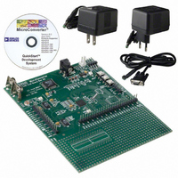
KIT DEV FOR ADUC832 QUICK START
Manufacturer
Analog Devices Inc
Series
QuickStart™ Kitr
Type
MCUr
Specifications of EVAL-ADUC832QSZ
Contents
Evaluation Board, Cable, Power Supply, Software and Documentation
Lead Free Status / RoHS Status
Lead free / RoHS Compliant
For Use With/related Products
ADuC832
Lead Free Status / RoHS Status
Compliant, Lead free / RoHS Compliant
Other names
EVAL-ADUC832QS
EVAL-ADUC832QS
EVAL-ADUC832QS


ADuC832
MEMORY ORGANIZATION
The ADuC832 contains four different memory blocks:
Flash/EE Program Memory
The ADuC832 provides 62 kBytes of Flash/EE program memory
to run user code. The user can choose to run code from this
internal memory or from an external program memory.
If the user applies power or resets the device while the EA pin is
pulled low, the part will execute code from the external program
space; otherwise the part defaults to code execution from its
internal 62 kBytes of Flash/EE program memory. Unlike the
ADuC812, where code execution can overflow from the internal
code space to external code space once the PC becomes greater
than 1FFFH, the ADuC832 does not support the rollover from
F7FFH in internal code space to F800H in external code space.
Instead the 2048 bytes between F800H and FFFFH will appear
as NOP instructions to user code.
This internal code space can be downloaded via the UART
serial port while the device is in-circuit. 56 kBytes of the program
memory can be reprogrammed during runtime; thus the code
space can be upgraded in the field using a user defined protocol
or it can be used as a data memory. This will be discussed in
more detail in the Flash/EE Memory section.
Flash/EE Data Memory
4 kBytes of Flash/EE data memory are available to the user
and can be accessed indirectly via a group of control registers
mapped into the Special Function Register (SFR) area. Access
to the Flash/EE data memory is discussed in detail later as part
of the Flash/EE Memory section.
General-Purpose RAM
The general-purpose RAM is divided into two separate memories,
namely the upper and the lower 128 bytes of RAM. The lower
128 bytes of RAM can be accessed through direct or indirect
addressing. The upper 128 bytes of RAM can only be accessed
through indirect addressing as it shares the same address space
as the SFR space, which can only be accessed through direct
addressing.
The lower 128 bytes of internal data memory are mapped as
shown in Figure 2. The lowest 32 bytes are grouped into four
banks of eight registers addressed as R0 through R7. The next
16 bytes (128 bits), locations 20H through 2FH above the
register banks, form a block of directly addressable bit locations
at bit addresses 00H through 7FH. The stack can be located
anywhere in the internal memory address space, and the stack
depth can be expanded up to 2048 bytes.
Reset initializes the stack pointer to location 07H and increments
it once before loading the stack to start from locations 08H
which is also the first register (R0) of register bank 1. Thus, if one
is going to use more than one register bank, the stack pointer
should be initialized to an area of RAM not used for data storage.
•
•
•
•
62 kBytes of On-Chip Flash/EE Program Memory
4 kBytes of On-Chip Flash/EE Data Memory
256 Bytes of General-Purpose RAM
2 kBytes of Internal XRAM
–14–
The ADuC832 contains 2048 bytes of internal XRAM, 1792 bytes
of which can be configured to be used as an extended 11-bit stack
pointer.
By default, the stack will operate exactly like an 8052 in that it
will roll over from FFH to 00H in the general-purpose RAM. On
the ADuC832, however, it is possible (by setting CFG832.7)
to enable the 11-bit extended stack pointer. In this case, the
stack will roll over from FFH in RAM to 0100H in XRAM.
The 11-bit stack pointer is visible in the SP and SPH SFRs.
The SP SFR is located at 81H as with a standard 8052. The
SPH SFR is located at B7H. The 3 LSBs of this SFR contain
the three extra bits necessary to extend the 8-bit stack pointer
into an 11-bit stack pointer.
Figure 2. Lower 128 Bytes of Internal Data Memory
BITS IN PSW
SELECTED
BANKS
VIA
Figure 3. Extended Stack Pointer Operation
CFG832.7 = 0
10
11
01
00
FFH
00H
30H
20H
18H
10H
08H
00H
ON-CHIP DATA
256 BYTES OF
(DATA +
STACK)
RAM
CFG832.7 = 1
07FFH
100H
00H
7FH
2FH
1FH
0FH
17H
07H
(DATA + STACK
ON-CHIP XRAM
ON-CHIP XRAM
FOR EXSP = 1,
FOR EXSP = 0)
(DATA ONLY)
UPPER 1792
DATA ONLY
LOWER 256
BYTES OF
BYTES OF
GENERAL-PURPOSE
AREA
BIT-ADDRESSABLE
(BIT ADDRESSES)
FOUR BANKS OF EIGHT
REGISTERS
R0 R7
RESET VALUE OF
STACK POINTER
REV. 0
Related parts for EVAL-ADUC832QSZ
Image
Part Number
Description
Manufacturer
Datasheet
Request
R


Part Number:
Description:
BOARD EVAL FOR SI270X-A
Manufacturer:
Silicon Laboratories Inc
Datasheet:

Part Number:
Description:
BUCK CONV REF DESIGN KIT IP1201
Manufacturer:
International Rectifier
Datasheet:
Part Number:
Description:
BOARD DEMO SYNC DUAL BUCK CNVTER
Manufacturer:
International Rectifier
Datasheet:
Part Number:
Description:
BOARD DEMO SYNC BUCK CONVETER
Manufacturer:
International Rectifier
Datasheet:

Part Number:
Description:
EVALBOARD/EB Omnidirectional microphone - Analog
Manufacturer:
Analog Devices
Datasheet:
Part Number:
Description:
EVALBOARD/EB Omnidirectional microphone - Analog
Manufacturer:
Analog Devices
Datasheet:


Part Number:
Description:
BOARD EVAL LED DRIVER LT3756
Manufacturer:
Linear Technology
Datasheet:

Part Number:
Description:
BOARD EVAL FOR AD7741/7742
Manufacturer:
Analog Devices Inc
Datasheet:

Part Number:
Description:
±1.7g Dual-Axis IMEMS Accelerometer Evaluation Board
Manufacturer:
Analog Devices Inc
Datasheet:

Part Number:
Description:
IC MULTIPLIER ANALOG 8-SOIC T/R
Manufacturer:
Analog Devices Inc
Datasheet:

Part Number:
Description:
IC ANALOG MULTIPLIER 8-DIP
Manufacturer:
Analog Devices Inc
Datasheet:
Part Number:
Description:
IC ANALOG MULTIPLIER 8-SOIC
Manufacturer:
Analog Devices Inc
Datasheet:
Part Number:
Description:
IC ANALOG MULTIPLIER 8-DIP
Manufacturer:
Analog Devices Inc
Datasheet: