EVAL-ADUC832QSZ Analog Devices Inc, EVAL-ADUC832QSZ Datasheet - Page 64
EVAL-ADUC832QSZ
Manufacturer Part Number
EVAL-ADUC832QSZ
Description
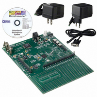
KIT DEV FOR ADUC832 QUICK START
Manufacturer
Analog Devices Inc
Series
QuickStart™ Kitr
Type
MCUr
Specifications of EVAL-ADUC832QSZ
Contents
Evaluation Board, Cable, Power Supply, Software and Documentation
Lead Free Status / RoHS Status
Lead free / RoHS Compliant
For Use With/related Products
ADuC832
Lead Free Status / RoHS Status
Compliant, Lead free / RoHS Compliant
Other names
EVAL-ADUC832QS
EVAL-ADUC832QS
EVAL-ADUC832QS


ADuC832
the oscillator, can also be enabled during power down. All other
on-chip peripherals however, are shut down. Port pins retain
their logic levels in this mode, but the DAC output goes to a
high impedance state (three-state). During full power-down
mode, the ADuC832 consumes a total of approximately 20 µA.
There are five ways of terminating power-down mode:
Asserting the RESET pin (Pin 15)
Returns to normal mode. All registers are set to their default
state and program execution starts at the reset vector once the
Reset pin is deasserted.
Cycling Power
All registers are set to their default state and program execution
starts at the reset vector approximately 128 ms later.
Time Interval Counter (TIC) Interrupt
Power-down mode is terminated and the CPU services the TIC
interrupt. The RETI at the end of the TIC ISR will return the
core to the instruction after the one that enabled power-down.
I
Power-down mode is terminated and the CPU services the
I
core to the instruction after the one that enabled power-down. It
should be noted that the I
bit (SERIPD) in the PCON SFR must first be set to allow this
mode of operation.
INT0 Interrupt
Power-down mode is terminated and the CPU services the
INT0 interrupt. The RETI at the end of the ISR will return the
core to the instruction after the one that enabled power-down.
The INT0 pin must not be driven low during or within 2 machine
cycles of the instruction that initiates power-down mode. It
should be noted that the INT0 power-down interrupt enable bit
(INT0PD) in the PCON SFR must first be set to allow this
mode of operation.
Power-On Reset
An internal POR (Power-On Reset) is implemented on the
ADuC832. For DV
the ADuC832 in reset. As DV
timer will timeout for 128 ms approximately before the part is
released from reset. The user must ensure that the power supply
has reached a stable 2.7 V minimum level by this time. Likewise
on power-down, the internal POR will hold the ADuC832 in
reset until the power supply has dropped below 1 V. Figure 62
illustrates the operation of the internal POR in detail.
Grounding and Board Layout Recommendations
As with all high resolution data converters, special attention
must be paid to grounding and PC board layout of ADuC832-
based designs in order to achieve optimum performance from
the ADC and DACs.
2
2
C/SPI interrupt. The RETI at the end of the ISR will return the
C or SPI Interrupt
DV
CORE RESET
INTERNAL
DD
2.45V TYP
1.0V TYP
Figure 62. Internal POR Operation
DD
128ms TYP
below 2.45 V, the internal POR will hold
2
C/SPI power-down interrupt enable
DD
rises above 2.45 V, an internal
128ms TYP
1.0V TYP
–64–
Although the ADuC832 has separate pins for analog and digital
ground (AGND and DGND), the user must not tie these to two
separate ground planes unless the two ground planes are connected
together very close to the ADuC832, as illustrated in the simpli-
fied example of Figure 63a. In systems where digital and analog
ground planes are connected together somewhere else (at the
system’s power supply for example), they cannot be connected
again near the ADuC832 since a ground loop would result. In
these cases, tie the ADuC832’s AGND and DGND pins all to
the analog ground plane, as illustrated in Figure 63b. In systems
with only one ground plane, ensure that the digital and analog
components are physically separated onto separate halves of the
board such that digital return currents do not flow near analog
circuitry and vice versa. The ADuC832 can then be placed between
the digital and analog sections, as illustrated in Figure 63c.
In all of these scenarios, and in more complicated real-life appli-
cations, keep in mind the flow of current from the supplies and
back to ground. Make sure the return paths for all currents are as
close as possible to the paths the currents took to reach their desti-
nations. For example, do not power components on the analog
side of Figure 63b with DV
from DV
currents flowing under analog circuitry, which could happen if
the user placed a noisy digital chip on the left half of the board
in Figure 63c. Whenever possible, avoid large discontinuities in
the ground plane(s) (such as are formed by a long trace on the
same layer), since they force return signals to travel a longer path.
And of course, make all connections to the ground plane directly,
with little or no trace separating the pin from its via to ground.
If the user plans to connect fast logic signals (rise/fall time < 5 ns)
to any of the ADuC832’s digital inputs, add a series resistor to
each relevant line to keep rise and fall times longer than 5 ns at
the ADuC832 input pins. A value of 100 Ω or 200 Ω is usually
sufficient to prevent high speed signals from coupling capacitively
into the ADuC832 and affecting the accuracy of ADC conversions.
b.
a.
c.
DD
Figure 63. System Grounding Schemes
to flow through AGND. Also, try to avoid digital
PLACE ANALOG
COMPONENTS
PLACE ANALOG
PLACE ANALOG
COMPONENTS
COMPONENTS
HERE
AGND
AGND
HERE
HERE
DD
since that would force return currents
GND
PLACE DIGITAL
COMPONENTS
PLACE DIGITAL
PLACE DIGITAL
COMPONENTS
COMPONENTS
HERE
HERE
HERE
DGND
DGND
REV. 0
Related parts for EVAL-ADUC832QSZ
Image
Part Number
Description
Manufacturer
Datasheet
Request
R


Part Number:
Description:
BOARD EVAL FOR SI270X-A
Manufacturer:
Silicon Laboratories Inc
Datasheet:

Part Number:
Description:
BUCK CONV REF DESIGN KIT IP1201
Manufacturer:
International Rectifier
Datasheet:
Part Number:
Description:
BOARD DEMO SYNC DUAL BUCK CNVTER
Manufacturer:
International Rectifier
Datasheet:
Part Number:
Description:
BOARD DEMO SYNC BUCK CONVETER
Manufacturer:
International Rectifier
Datasheet:

Part Number:
Description:
EVALBOARD/EB Omnidirectional microphone - Analog
Manufacturer:
Analog Devices
Datasheet:
Part Number:
Description:
EVALBOARD/EB Omnidirectional microphone - Analog
Manufacturer:
Analog Devices
Datasheet:


Part Number:
Description:
BOARD EVAL LED DRIVER LT3756
Manufacturer:
Linear Technology
Datasheet:

Part Number:
Description:
BOARD EVAL FOR AD7741/7742
Manufacturer:
Analog Devices Inc
Datasheet:

Part Number:
Description:
±1.7g Dual-Axis IMEMS Accelerometer Evaluation Board
Manufacturer:
Analog Devices Inc
Datasheet:

Part Number:
Description:
IC MULTIPLIER ANALOG 8-SOIC T/R
Manufacturer:
Analog Devices Inc
Datasheet:

Part Number:
Description:
IC ANALOG MULTIPLIER 8-DIP
Manufacturer:
Analog Devices Inc
Datasheet:
Part Number:
Description:
IC ANALOG MULTIPLIER 8-SOIC
Manufacturer:
Analog Devices Inc
Datasheet:
Part Number:
Description:
IC ANALOG MULTIPLIER 8-DIP
Manufacturer:
Analog Devices Inc
Datasheet: