EVAL-ADUC832QSZ Analog Devices Inc, EVAL-ADUC832QSZ Datasheet - Page 65
EVAL-ADUC832QSZ
Manufacturer Part Number
EVAL-ADUC832QSZ
Description
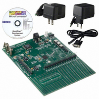
KIT DEV FOR ADUC832 QUICK START
Manufacturer
Analog Devices Inc
Series
QuickStart™ Kitr
Type
MCUr
Specifications of EVAL-ADUC832QSZ
Contents
Evaluation Board, Cable, Power Supply, Software and Documentation
Lead Free Status / RoHS Status
Lead free / RoHS Compliant
For Use With/related Products
ADuC832
Lead Free Status / RoHS Status
Compliant, Lead free / RoHS Compliant
Other names
EVAL-ADUC832QS
EVAL-ADUC832QS
EVAL-ADUC832QS


OTHER HARDWARE CONSIDERATIONS
To facilitate in-circuit programming, plus in-circuit debug and
emulation options, users will want to implement some simple
connection points in their hardware that will allow easy access
to download, debug, and emulation modes.
In-Circuit Serial Download Access
Nearly all ADuC832 designs will want to take advantage of the
in-circuit reprogrammability of the chip. This is accomplished by
a connection to the ADuC832’s UART, which requires an
external RS-232 chip for level translation if downloading code
from a PC. Basic configuration of an RS-232 connection is
illustrated in Figure 64 with a simple ADM202-based circuit.
If users would rather not design an RS-232 chip onto a board,
refer to the application note “uC006–A 4-Wire UART-to-PC
Interface”* for a simple (and zero-cost-per-board) method of
gaining in-circuit serial download access to the ADuC832.
REV. 0
*Application Note uC006 is available at
ANALOG INPUT
V
DAC OUTPUT
REF
OUTPUT
www.analog.com/microconverter
Figure 64. Example ADuC832 System (PQFP Package)
AV
C1+
V+
C1–
C2+
C2–
V–
T2OUT
R2IN
DD
ADM202
R1OUT
R2OUT
T1OUT
GND
R1IN
T1IN
T2IN
V
CC
10
ADC0
AV
AGND
C REF
V REF
DAC0
DAC1
52
14
DD
DV
51
DD
50
16
–65–
49
DV
18
In addition to the basic UART connections, users will also need a
way to trigger the chip into download mode. This is accomplished
via a 1 kΩ pull-down resistor that can be jumpered onto the PSEN
pin, as shown in Figure 64. To get the ADuC832 into download
mode, simply connect this jumper and power-cycle the device
(or manually reset the device, if a manual reset button is available)
and it will be ready to receive a new program serially. With the
jumper removed, the device will come up in normal mode (and
run the program) whenever power is cycled or RESET is toggled.
Note that PSEN is normally an output (as described in the
External Memory Interface section) and is sampled as an input
only on the falling edge of RESET (i.e., at power-up or upon an
external manual reset). Note also that if any external circuitry
unintentionally pulls PSEN low during power-up or reset events,
it could cause the chip to enter download mode and therefore
fail to begin user code execution as it should. To prevent this,
ensure that no external signals are capable of pulling the PSEN
pin low, except for the external PSEN jumper itself.
48
DD
DV
ADuC832
19
47
DD
20
9-PIN D-SUB
46
FEMALE
45
DOWNLOAD/DEBUG
(NORMALLY OPEN)
1
2
3
4
5
6
7
8
9
44 43
ENABLE JUMPER
1k
24
42
NOT CONNECTED IN THIS EXAMPLE
41
XTAL2
XTAL1
DGND
DV
26
1k
40
DD
DV
39
38
37
36
35
34
33
32
31
30
29
28
27
DD
32.768kHz
DV
DD
2-PIN HEADER FOR
EMULATION ACCESS
(NORMALLY OPEN)
ADuC832
Related parts for EVAL-ADUC832QSZ
Image
Part Number
Description
Manufacturer
Datasheet
Request
R


Part Number:
Description:
BOARD EVAL FOR SI270X-A
Manufacturer:
Silicon Laboratories Inc
Datasheet:

Part Number:
Description:
BUCK CONV REF DESIGN KIT IP1201
Manufacturer:
International Rectifier
Datasheet:
Part Number:
Description:
BOARD DEMO SYNC DUAL BUCK CNVTER
Manufacturer:
International Rectifier
Datasheet:
Part Number:
Description:
BOARD DEMO SYNC BUCK CONVETER
Manufacturer:
International Rectifier
Datasheet:

Part Number:
Description:
EVALBOARD/EB Omnidirectional microphone - Analog
Manufacturer:
Analog Devices
Datasheet:
Part Number:
Description:
EVALBOARD/EB Omnidirectional microphone - Analog
Manufacturer:
Analog Devices
Datasheet:


Part Number:
Description:
BOARD EVAL LED DRIVER LT3756
Manufacturer:
Linear Technology
Datasheet:

Part Number:
Description:
BOARD EVAL FOR AD7741/7742
Manufacturer:
Analog Devices Inc
Datasheet:

Part Number:
Description:
±1.7g Dual-Axis IMEMS Accelerometer Evaluation Board
Manufacturer:
Analog Devices Inc
Datasheet:

Part Number:
Description:
IC MULTIPLIER ANALOG 8-SOIC T/R
Manufacturer:
Analog Devices Inc
Datasheet:

Part Number:
Description:
IC ANALOG MULTIPLIER 8-DIP
Manufacturer:
Analog Devices Inc
Datasheet:
Part Number:
Description:
IC ANALOG MULTIPLIER 8-SOIC
Manufacturer:
Analog Devices Inc
Datasheet:
Part Number:
Description:
IC ANALOG MULTIPLIER 8-DIP
Manufacturer:
Analog Devices Inc
Datasheet: