EVAL-ADUC832QSZ Analog Devices Inc, EVAL-ADUC832QSZ Datasheet - Page 61
EVAL-ADUC832QSZ
Manufacturer Part Number
EVAL-ADUC832QSZ
Description
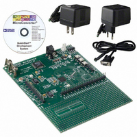
KIT DEV FOR ADUC832 QUICK START
Manufacturer
Analog Devices Inc
Series
QuickStart™ Kitr
Type
MCUr
Specifications of EVAL-ADUC832QSZ
Contents
Evaluation Board, Cable, Power Supply, Software and Documentation
Lead Free Status / RoHS Status
Lead free / RoHS Compliant
For Use With/related Products
ADuC832
Lead Free Status / RoHS Status
Compliant, Lead free / RoHS Compliant
Other names
EVAL-ADUC832QS
EVAL-ADUC832QS
EVAL-ADUC832QS


Interrupt Priority
The Interrupt Enable registers are written by the user to enable
individual interrupt sources, while the Interrupt Priority registers
allow the user to select one of two priority levels for each interrupt.
An interrupt of a high priority may interrupt the service routine
of a low priority interrupt, and if two interrupts of different priority
occur at the same time, the higher level interrupt will be serviced
first. An interrupt cannot be interrupted by another interrupt of
the same priority level. If two interrupts of the same priority level
occur simultaneously, a polling sequence is observed as shown
in Table XXXII.
Source
PSMI
WDS
IE0
ADCI
TF0
IE1
TF1
ISPI/I2CI
RI + TI
TF2 + EXF2
TII
Interrupt Vectors
When an interrupt occurs, the program counter is pushed onto
the stack and the corresponding interrupt vector address is loaded
into the program counter. The Interrupt Vector Addresses are
shown in Table XXXIII.
REV. 0
Table XXXII. Priority within an Interrupt Level
Source
IE0
TF0
IE1
TF1
RI + TI
TF2 + EXF2
ADCI
ISPI/I2CI
PSMI
TII
WDS
Table XXXIII. Interrupt Vector Addresses
Priority
1 (Highest)
2
2
3
4
5
6
7
8
9 (Lowest)
11(Lowest)
Description
Power Supply Monitor Interrupt
Watchdog Timer Interrupt
External Interrupt 0
ADC Interrupt
Timer/Counter 0 Interrupt
External Interrupt 1
Timer/Counter 1 Interrupt
SPI Interrupt/I
Serial Interrupt
Timer/Counter 2 Interrupt
Time Interval Counter Interrupt
0003H
000BH
0013H
001BH
0023H
002BH
0033H
003BH
0043H
0053H
005BH
Vector Address
2
C Interrupt
–61–
ADuC832 HARDWARE DESIGN CONSIDERATIONS
This section outlines some of the key hardware design consider-
ations that must be addressed when integrating the ADuC832
into any hardware system.
Clock Oscillator
The clock source for the ADuC832 can be generated by the
internal PLL or by an external clock input. To use the internal
PLL, connect a 32.768 kHz parallel resonant crystal between
XTAL1 and XTAL2, and connect a capacitor from each pin to
ground as shown below. This crystal allows the PLL to lock cor-
rectly to give a f
the PLL will free run, giving a f
useful if an external clock input is required. The part will power
up and the PLL will free run; the user then in software writes to
the CFG832 SFR to enable the external clock input on P3.4.
Whether using the internal PLL or an external clock source, the
ADuC832’s specified operational clock speed range is 400 kHz to
16.777216 MHz. The core itself is static, and will function all
the way down to dc. But at clock speeds slower that 400 kHz, the
ADC will no longer function correctly. Therefore, to ensure
specified operation, use a clock frequency of at least 400 kHz and
no more than 16.777216 MHz.
Figure 55. External Parallel Resonant Crystal Connections
Figure 56. Connecting an External Clock Source
EXTERNAL
SOURCE
CLOCK
VCO
XTAL1
XTAL2
of 16.777216 MHz. If no crystal is present,
P3.4
VCO
of 16.7 MHz 20%. This is
ADuC832
ADuC832
TO INTERNAL
TIMING CIRCUITS
TO INTERNAL
TIMING CIRCUITS
ADuC832
Related parts for EVAL-ADUC832QSZ
Image
Part Number
Description
Manufacturer
Datasheet
Request
R


Part Number:
Description:
BOARD EVAL FOR SI270X-A
Manufacturer:
Silicon Laboratories Inc
Datasheet:

Part Number:
Description:
BUCK CONV REF DESIGN KIT IP1201
Manufacturer:
International Rectifier
Datasheet:
Part Number:
Description:
BOARD DEMO SYNC DUAL BUCK CNVTER
Manufacturer:
International Rectifier
Datasheet:
Part Number:
Description:
BOARD DEMO SYNC BUCK CONVETER
Manufacturer:
International Rectifier
Datasheet:

Part Number:
Description:
EVALBOARD/EB Omnidirectional microphone - Analog
Manufacturer:
Analog Devices
Datasheet:
Part Number:
Description:
EVALBOARD/EB Omnidirectional microphone - Analog
Manufacturer:
Analog Devices
Datasheet:


Part Number:
Description:
BOARD EVAL LED DRIVER LT3756
Manufacturer:
Linear Technology
Datasheet:

Part Number:
Description:
BOARD EVAL FOR AD7741/7742
Manufacturer:
Analog Devices Inc
Datasheet:

Part Number:
Description:
±1.7g Dual-Axis IMEMS Accelerometer Evaluation Board
Manufacturer:
Analog Devices Inc
Datasheet:

Part Number:
Description:
IC MULTIPLIER ANALOG 8-SOIC T/R
Manufacturer:
Analog Devices Inc
Datasheet:

Part Number:
Description:
IC ANALOG MULTIPLIER 8-DIP
Manufacturer:
Analog Devices Inc
Datasheet:
Part Number:
Description:
IC ANALOG MULTIPLIER 8-SOIC
Manufacturer:
Analog Devices Inc
Datasheet:
Part Number:
Description:
IC ANALOG MULTIPLIER 8-DIP
Manufacturer:
Analog Devices Inc
Datasheet: