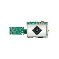
MCIMX35WPDKJ Freescale Semiconductor, MCIMX35WPDKJ Datasheet - Page 104

MCIMX35WPDKJ
Manufacturer Part Number
MCIMX35WPDKJ
Description
BOARD DEV FOR I.MX35
Manufacturer
Freescale Semiconductor
Series
i.MX35r
Type
MPUr
Datasheets
1.MCIMX35WPDKJ.pdf
(148 pages)
2.MCIMX35WPDKJ.pdf
(2 pages)
3.MCIMX35WPDKJ.pdf
(10 pages)
Specifications of MCIMX35WPDKJ
Contents
Module and Misc Hardware
Processor To Be Evaluated
i.MX35
Processor Series
i.MX35
Data Bus Width
32 bit
Interface Type
RS-232, Ethernet, USB, CAN, JTAG
Core
ARM11
For Use With/related Products
i.MX35
Lead Free Status / RoHS Status
Lead free / RoHS Compliant
- Current page: 104 of 148
- Download datasheet (3Mb)
Figure 78
timing parameters for MDMA read and write.
104
Parameter
tg(write)
tg(read)
tf(write)
tf(read)
tm, ti
ATA
td
t0
tL
tk
shows timing for MDMA read, and
Parameter
Figure
Figure 79
td, td1
i.MX35 Applications Processors for Industrial and Consumer Products, Rev. 9
from
tgr
tm
—
tfr
—
—
—
tk
78,
Table 68. MDMA Read and Write Timing Parameters
tm (min.) = ti (min.) = time_m × T – (tskew1 + tskew2 + tskew5)
td1.(min.) = td (min.) = time_d × T – (tskew1 + tskew2 + tskew6)
tk.(min.) = time_k × T – (tskew1 + tskew2 + tskew6)
t0 (min.) = (time_d + time_k) × T
tgr (min. – read) = tco + tsu + tbuf + tbuf + tcable1 + tcable2
tgr.(min. – drive) = td – te(drive)
tfr (min. – drive) = 0
tg (min. – write) = time_d × T – (tskew1 + tskew2 + tskew5)
tf (min. – write) = time_k × T – (tskew1 + tskew2 + tskew6)
tL (max.) = (time_d + time_k–2) × T – (tsu + tco + 2 × tbuf + 2 × tcable2)
Figure 78. MDMA Read Timing Diagram
Figure 79. MDMA Write Timing Diagram
Figure 79
shows timing for MDMA write.
Value
Freescale Semiconductor
Table 68
time_d, time_k
time_d, time_k
Controlling
Variable
time_m
time_d
time_d
time_d
time_k
time_k
lists the
—
Related parts for MCIMX35WPDKJ
Image
Part Number
Description
Manufacturer
Datasheet
Request
R
Part Number:
Description:
MCIMX-LVDS1
Manufacturer:
Freescale Semiconductor
Datasheet:
Part Number:
Description:
Manufacturer:
Freescale Semiconductor, Inc
Datasheet:
Part Number:
Description:
Manufacturer:
Freescale Semiconductor, Inc
Datasheet:
Part Number:
Description:
Manufacturer:
Freescale Semiconductor, Inc
Datasheet:
Part Number:
Description:
Manufacturer:
Freescale Semiconductor, Inc
Datasheet:
Part Number:
Description:
Manufacturer:
Freescale Semiconductor, Inc
Datasheet:
Part Number:
Description:
Manufacturer:
Freescale Semiconductor, Inc
Datasheet:
Part Number:
Description:
Manufacturer:
Freescale Semiconductor, Inc
Datasheet:
Part Number:
Description:
Manufacturer:
Freescale Semiconductor, Inc
Datasheet:
Part Number:
Description:
Manufacturer:
Freescale Semiconductor, Inc
Datasheet:
Part Number:
Description:
Manufacturer:
Freescale Semiconductor, Inc
Datasheet:
Part Number:
Description:
Manufacturer:
Freescale Semiconductor, Inc
Datasheet:
Part Number:
Description:
Manufacturer:
Freescale Semiconductor, Inc
Datasheet:
Part Number:
Description:
Manufacturer:
Freescale Semiconductor, Inc
Datasheet:
Part Number:
Description:
Manufacturer:
Freescale Semiconductor, Inc
Datasheet:


