MCIMX35WPDKJ Freescale Semiconductor, MCIMX35WPDKJ Datasheet - Page 61

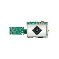
MCIMX35WPDKJ
Manufacturer Part Number
MCIMX35WPDKJ
Description
BOARD DEV FOR I.MX35
Manufacturer
Freescale Semiconductor
Series
i.MX35r
Type
MPUr
Datasheets
1.MCIMX35WPDKJ.pdf
(148 pages)
2.MCIMX35WPDKJ.pdf
(2 pages)
3.MCIMX35WPDKJ.pdf
(10 pages)
Specifications of MCIMX35WPDKJ
Contents
Module and Misc Hardware
Processor To Be Evaluated
i.MX35
Processor Series
i.MX35
Data Bus Width
32 bit
Interface Type
RS-232, Ethernet, USB, CAN, JTAG
Core
ARM11
For Use With/related Products
i.MX35
Lead Free Status / RoHS Status
Lead free / RoHS Compliant
- Current page: 61 of 148
- Download datasheet (3Mb)
4.9.8
This section describes the electrical information of the FEC module. The FEC is designed to support both
10- and 100-Mbps Ethernet networks. An external transceiver interface and transceiver function are
required to complete the interface to the media. The FEC supports the 10/100 Mbps Media Independent
Interface (MII) using a total of 18 pins. The 10-Mbps 7-wire interface that is restricted to a 10-Mbps data
rate uses seven of the MII pins for connection to an external Ethernet transceiver.
4.9.8.1
This section describes the AC timing specifications of the FEC. The MII signals are compatible with
transceivers operating at a voltage of 3.3 V.
4.9.8.2
The MII receive timing signals consist of FEC_RXD[3:0], FEC_RX_DV, FEC_RX_ER, and
FEC_RX_CLK. The receiver functions correctly up to a FEC_RX_CLK maximum frequency of
25 MHz + 1%. There is no minimum frequency requirement. Additionally, the processor clock frequency
must exceed twice the FEC_RX_CLK frequency.
1
Figure 40
Freescale Semiconductor
FEC_RX_DV, FEC_RX_CLK, and FEC_RXD0 have the same timing when in 10 Mbps 7-wire interface mode.
Num.
M1
M2
M3
M4
FEC_RXD[3:0], FEC_RX_DV, FEC_RX_ER to FEC_RX_CLK setup
FEC_RX_CLK to FEC_RXD[3:0], FEC_RX_DV, FEC_RX_ER hold
FEC_RX_CLK pulse width high
FEC_RX_CLK pulse width low
FEC_RXD[3:0] (inputs)
FEC_RX_CLK (input)
shows the MII receive signal timings listed in
Fast Ethernet Controller (FEC) AC Electrical Specifications
FEC AC Timing
MII Receive Signal Timing
FEC_RX_ER
FEC_RX_DV
i.MX35 Applications Processors for Industrial and Consumer Products, Rev. 9
Figure 40. MII Receive Signal Timing Diagram
Characteristic
Table 45. MII Receive Signal Timing
M1
1
M2
Table 45
M3
Table
lists MII receive channel timings.
45.
Min.
35%
35%
5
5
M4
Max.
65%
65%
—
—
FEC_RX_CLK period
FEC_RX_CLK period
Unit
ns
ns
61
Related parts for MCIMX35WPDKJ
Image
Part Number
Description
Manufacturer
Datasheet
Request
R
Part Number:
Description:
MCIMX-LVDS1
Manufacturer:
Freescale Semiconductor
Datasheet:
Part Number:
Description:
Manufacturer:
Freescale Semiconductor, Inc
Datasheet:
Part Number:
Description:
Manufacturer:
Freescale Semiconductor, Inc
Datasheet:
Part Number:
Description:
Manufacturer:
Freescale Semiconductor, Inc
Datasheet:
Part Number:
Description:
Manufacturer:
Freescale Semiconductor, Inc
Datasheet:
Part Number:
Description:
Manufacturer:
Freescale Semiconductor, Inc
Datasheet:
Part Number:
Description:
Manufacturer:
Freescale Semiconductor, Inc
Datasheet:
Part Number:
Description:
Manufacturer:
Freescale Semiconductor, Inc
Datasheet:
Part Number:
Description:
Manufacturer:
Freescale Semiconductor, Inc
Datasheet:
Part Number:
Description:
Manufacturer:
Freescale Semiconductor, Inc
Datasheet:
Part Number:
Description:
Manufacturer:
Freescale Semiconductor, Inc
Datasheet:
Part Number:
Description:
Manufacturer:
Freescale Semiconductor, Inc
Datasheet:
Part Number:
Description:
Manufacturer:
Freescale Semiconductor, Inc
Datasheet:
Part Number:
Description:
Manufacturer:
Freescale Semiconductor, Inc
Datasheet:
Part Number:
Description:
Manufacturer:
Freescale Semiconductor, Inc
Datasheet:


