MCIMX35WPDKJ Freescale Semiconductor, MCIMX35WPDKJ Datasheet - Page 110
MCIMX35WPDKJ
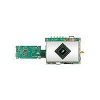
Manufacturer Part Number
MCIMX35WPDKJ
Description
BOARD DEV FOR I.MX35
Manufacturer
Freescale Semiconductor
Series
i.MX35r
Type
MPUr
Datasheets
1.MCIMX35WPDKJ.pdf
(148 pages)
2.MCIMX35WPDKJ.pdf
(2 pages)
3.MCIMX35WPDKJ.pdf
(10 pages)
Specifications of MCIMX35WPDKJ
Contents
Module and Misc Hardware
Processor To Be Evaluated
i.MX35
Processor Series
i.MX35
Data Bus Width
32 bit
Interface Type
RS-232, Ethernet, USB, CAN, JTAG
Core
ARM11
For Use With/related Products
i.MX35
Lead Free Status / RoHS Status
Lead free / RoHS Compliant


pin. The modulated signal of the module is observed at this pin. It can be viewed as a clock signal whose
period and duty cycle can be varied with different settings of the PWM. The smallest period is two ipg_clk
periods with duty cycle of 50 percent.
4.9.20
This section details the electrical characteristics for the SJC module.
input timing.
Figure 90
110
depicts the SJC TRST timing, and
Outputs
Outputs
Outputs
SJC Electrical Specifications
(Input)
(Input)
Inputs
Figure 88
TCK
Data
Data
Data
Data
TCK
i.MX35 Applications Processors for Industrial and Consumer Products, Rev. 9
depicts the SJC boundary scan timing,
VIL
SJ3
Figure 88. Boundary Scan (JTAG) Timing Diagram
Figure 87. Test Clock Input Timing Diagram
VIH
SJ7
SJ6
SJ6
VIL
Table 73
VM
SJ2
lists the SJC timing parameters.
Output Data Valid
Output Data Valid
SJ1
SJ4
Input Data Valid
Figure 89
Figure 87
SJ3
SJ2
VM
VIH
depicts the SJC test access port,
SJ5
depicts the SJC test clock
Freescale Semiconductor
Related parts for MCIMX35WPDKJ
Image
Part Number
Description
Manufacturer
Datasheet
Request
R

Part Number:
Description:
MCIMX-LVDS1
Manufacturer:
Freescale Semiconductor
Datasheet:

Part Number:
Description:
Manufacturer:
Freescale Semiconductor, Inc
Datasheet:
Part Number:
Description:
Manufacturer:
Freescale Semiconductor, Inc
Datasheet:
Part Number:
Description:
Manufacturer:
Freescale Semiconductor, Inc
Datasheet:
Part Number:
Description:
Manufacturer:
Freescale Semiconductor, Inc
Datasheet:
Part Number:
Description:
Manufacturer:
Freescale Semiconductor, Inc
Datasheet:
Part Number:
Description:
Manufacturer:
Freescale Semiconductor, Inc
Datasheet:
Part Number:
Description:
Manufacturer:
Freescale Semiconductor, Inc
Datasheet:
Part Number:
Description:
Manufacturer:
Freescale Semiconductor, Inc
Datasheet:
Part Number:
Description:
Manufacturer:
Freescale Semiconductor, Inc
Datasheet:
Part Number:
Description:
Manufacturer:
Freescale Semiconductor, Inc
Datasheet:
Part Number:
Description:
Manufacturer:
Freescale Semiconductor, Inc
Datasheet:
Part Number:
Description:
Manufacturer:
Freescale Semiconductor, Inc
Datasheet:
Part Number:
Description:
Manufacturer:
Freescale Semiconductor, Inc
Datasheet:
Part Number:
Description:
Manufacturer:
Freescale Semiconductor, Inc
Datasheet: