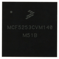
MCF5253CVM140 Freescale Semiconductor, MCF5253CVM140 Datasheet - Page 102

MCF5253CVM140
Manufacturer Part Number
MCF5253CVM140
Description
IC MPU 32BIT 140MHZ 225-MAPBGA
Manufacturer
Freescale Semiconductor
Series
MCF525xr
Datasheets
1.MCF5253VM140J.pdf
(34 pages)
2.MCF5253VM140J.pdf
(8 pages)
3.MCF5253VM140J.pdf
(648 pages)
4.MCF5253VM140J.pdf
(2 pages)
Specifications of MCF5253CVM140
Core Processor
Coldfire V2
Core Size
32-Bit
Speed
140MHz
Connectivity
CAN, EBI/EMI, I²C, QSPI, UART/USART, USB OTG
Peripherals
DMA, WDT
Program Memory Type
ROMless
Ram Size
128K x 8
Voltage - Supply (vcc/vdd)
1.08 V ~ 1.32 V
Data Converters
A/D 6x12b
Oscillator Type
External
Operating Temperature
-40°C ~ 85°C
Package / Case
225-MAPBGA
Family Name
MCF5xxx
Device Core
ColdFire V2
Device Core Size
32b
Frequency (max)
140MHz
Instruction Set Architecture
RISC
Supply Voltage 1 (typ)
1.2/3.3V
Operating Supply Voltage (max)
1.32/3.6V
Operating Supply Voltage (min)
1.08/3V
Operating Temp Range
-40C to 85C
Operating Temperature Classification
Industrial
Mounting
Surface Mount
Pin Count
225
Package Type
MA-BGA
Lead Free Status / RoHS Status
Lead free / RoHS Compliant
Number Of I /o
-
Eeprom Size
-
Program Memory Size
-
Lead Free Status / Rohs Status
Compliant
Available stocks
Company
Part Number
Manufacturer
Quantity
Price
Company:
Part Number:
MCF5253CVM140
Manufacturer:
FREESCALE
Quantity:
300
Company:
Part Number:
MCF5253CVM140
Manufacturer:
Freescale Semiconductor
Quantity:
10 000
Part Number:
MCF5253CVM140
Manufacturer:
FREESCALE
Quantity:
20 000
Company:
Part Number:
MCF5253CVM140J
Manufacturer:
Freescale Semiconductor
Quantity:
10 000
- MCF5253VM140J PDF datasheet
- MCF5253VM140J PDF datasheet #2
- MCF5253VM140J PDF datasheet #3
- MCF5253VM140J PDF datasheet #4
- Current page: 102 of 648
- Download datasheet (8Mb)
Static RAM (SRAM)
6.3.2
After a hardware reset, the contents of the SRAM module are undefined. The valid bit of the RAMBAR
is cleared, disabling the module. If the SRAM requires initialization with instructions or data, the
following steps should be performed:
The ColdFire processor or an external emulator using the debug module can perform these initialization
functions.
6.3.3
The following code segment describes how to initialize the SRAM. The code sets the base address of the
SRAM at $20000000 and then initializes the RAM to zeros.
RAMBASE EQU $20000000; set this variable to $20000000
RAMVALID EQU $00000001;
move.l #RAMBASE+RAMVALID,D0;load RAMBASE + valid bit into D0.
movec.l D0, RAMBAR;load RAMBAR and enable SRAM
The following loop initializes the entire SRAM to zero
lea.l RAMBASE,A0;load pointer to SRAM
move.l #4096,D0;load loop counter into D0
SRAM_INIT_LOOP:
clr.l (A0)+); clear 4 bytes of SRAM
subq.l #1,D0;decrement loop counter
bne.b SRAM_INIT_LOOP;if done, then exit; else continue looping
6.3.4
As noted previously, depending on the configuration defined by the RAMBAR, instruction fetch and
operand read accesses may be sent to the SRAM and unified cache simultaneously. If the access is mapped
to the SRAM module, it sources the read data, and the unified cache access is discarded. If the SRAM is
used only for data operands, asserting the ASn bits associated with instruction fetches can decrease power
dissipation. Additionally, if the SRAM contains only instructions, masking data accesses can reduce power
dissipation.
6-4
1. Load the RAMBAR mapping the SRAM module to the desired location within the address space
2. Read the source data and write it to the SRAM. There are various instructions to support this
3. After the data has been loaded into the SRAM, it may be appropriate to load a revised value into
and set the Valid bit.
function, including memory-to-memory move instructions, or the MOVEM opcode. The MOVEM
instruction is optimized to generate line-sized burst fetches on modulo-64 addresses, so this opcode
generally provides maximum performance.
the RAMBAR with a new set of attributes. These attributes consist of the write-protect and address
space mask fields.
SRAM Initialization
SRAM Initialization Code
Power Management
Table 6-2
shows some examples of typical RAMBAR settings.
MCF5253 Reference Manual, Rev. 1
Freescale Semiconductor
Related parts for MCF5253CVM140
Image
Part Number
Description
Manufacturer
Datasheet
Request
R
Part Number:
Description:
Mcf5253 Coldfire? Microprocessor Data Sheet
Manufacturer:
Freescale Semiconductor, Inc
Datasheet:
Part Number:
Description:
Manufacturer:
Freescale Semiconductor, Inc
Datasheet:
Part Number:
Description:
Manufacturer:
Freescale Semiconductor, Inc
Datasheet:
Part Number:
Description:
Manufacturer:
Freescale Semiconductor, Inc
Datasheet:
Part Number:
Description:
Manufacturer:
Freescale Semiconductor, Inc
Datasheet:
Part Number:
Description:
Manufacturer:
Freescale Semiconductor, Inc
Datasheet:
Part Number:
Description:
Manufacturer:
Freescale Semiconductor, Inc
Datasheet:
Part Number:
Description:
Manufacturer:
Freescale Semiconductor, Inc
Datasheet:
Part Number:
Description:
Manufacturer:
Freescale Semiconductor, Inc
Datasheet:
Part Number:
Description:
Manufacturer:
Freescale Semiconductor, Inc
Datasheet:
Part Number:
Description:
Manufacturer:
Freescale Semiconductor, Inc
Datasheet:
Part Number:
Description:
Manufacturer:
Freescale Semiconductor, Inc
Datasheet:
Part Number:
Description:
Manufacturer:
Freescale Semiconductor, Inc
Datasheet:
Part Number:
Description:
Manufacturer:
Freescale Semiconductor, Inc
Datasheet:
Part Number:
Description:
Manufacturer:
Freescale Semiconductor, Inc
Datasheet:


