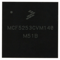
MCF5253CVM140 Freescale Semiconductor, MCF5253CVM140 Datasheet - Page 120

MCF5253CVM140
Manufacturer Part Number
MCF5253CVM140
Description
IC MPU 32BIT 140MHZ 225-MAPBGA
Manufacturer
Freescale Semiconductor
Series
MCF525xr
Datasheets
1.MCF5253VM140J.pdf
(34 pages)
2.MCF5253VM140J.pdf
(8 pages)
3.MCF5253VM140J.pdf
(648 pages)
4.MCF5253VM140J.pdf
(2 pages)
Specifications of MCF5253CVM140
Core Processor
Coldfire V2
Core Size
32-Bit
Speed
140MHz
Connectivity
CAN, EBI/EMI, I²C, QSPI, UART/USART, USB OTG
Peripherals
DMA, WDT
Program Memory Type
ROMless
Ram Size
128K x 8
Voltage - Supply (vcc/vdd)
1.08 V ~ 1.32 V
Data Converters
A/D 6x12b
Oscillator Type
External
Operating Temperature
-40°C ~ 85°C
Package / Case
225-MAPBGA
Family Name
MCF5xxx
Device Core
ColdFire V2
Device Core Size
32b
Frequency (max)
140MHz
Instruction Set Architecture
RISC
Supply Voltage 1 (typ)
1.2/3.3V
Operating Supply Voltage (max)
1.32/3.6V
Operating Supply Voltage (min)
1.08/3V
Operating Temp Range
-40C to 85C
Operating Temperature Classification
Industrial
Mounting
Surface Mount
Pin Count
225
Package Type
MA-BGA
Lead Free Status / RoHS Status
Lead free / RoHS Compliant
Number Of I /o
-
Eeprom Size
-
Program Memory Size
-
Lead Free Status / Rohs Status
Compliant
Available stocks
Company
Part Number
Manufacturer
Quantity
Price
Company:
Part Number:
MCF5253CVM140
Manufacturer:
FREESCALE
Quantity:
300
Company:
Part Number:
MCF5253CVM140
Manufacturer:
Freescale Semiconductor
Quantity:
10 000
Part Number:
MCF5253CVM140
Manufacturer:
FREESCALE
Quantity:
20 000
Company:
Part Number:
MCF5253CVM140J
Manufacturer:
Freescale Semiconductor
Quantity:
10 000
- MCF5253VM140J PDF datasheet
- MCF5253VM140J PDF datasheet #2
- MCF5253VM140J PDF datasheet #3
- MCF5253VM140J PDF datasheet #4
- Current page: 120 of 648
- Download datasheet (8Mb)
Synchronous DRAM Controller Module
7.5
Synchronous DRAMs have a prescribed initialization sequence. The DRAM controller supports this
sequence with the following procedure:
7.5.1
It is possible to configure the operation of SDRAMs, namely their burst operation and CAS latency,
through the SDRAM mode register. CAS latency is a function of the speed of the SDRAM and the bus
clock of the DRAM controller. The DRAM controller operates at a CAS latency of 1 or 2.
Although the MCF5253 DRAM controller supports bursting operations, it does not use the bursting
features of the SDRAMs. Because the MCF5253 can burst operand sizes of 1, 2, 4, or 16 bytes long, the
concept of a fixed burst length in the SDRAMs mode register becomes problematic. Therefore, the
MCF5253 DRAM controller generates the burst cycles rather than the SDRAM device. Because the
MCF5253 generates a new address and a
SDRAM mode register should be set either to a burst length of one or to not burst. This allows bursting to
be controlled by the MCF5253 instead.
The SDRAM mode register is written to by setting the associated block’s DACR[IMRS]. First, the base
address and mask registers must be set to the appropriate configuration to allow the mode register to be set.
7-16
1. SDRAM control signals are reset to idle state. Wait the prescribed period after reset before any
2. Initialize the DCR, DACR, and DMR in their operational configuration. Do not yet enable
3. Issue a
4. Enable refresh (set DACR[RE]) and wait for at least 8 refreshes to occur.
5. Before issuing the
6. Issue the
action is taken on the SDRAMs. This is normally around 100 µs.
REF
Wait the time (determined by t
the
Initialization Sequence
MRS
commands.
Mode Register Settings
PALL
Mode register settings are driven on the SDRAM address bus, so care must
be taken to change DMR[BAM] if the mode register configuration does not
fall in the address range determined by the address mask bits. After the
mode register is set, DMR mask bits can be restored to their desired
configuration.
Improperly set DMR mask bits may prevent access to the mode register
address. Thus, the user should determine the mapping of the mode register
address to the MCF5253 address bits to find out if an access is blocked. If
the DMR setting prohibits mode register access, the DMR should be
reconfigured to enable the access and then set to its necessary configuration
after the
to execute properly.
MRS
command to the SDRAMs by setting DCR[IP] and accessing a SDRAM location.
command by setting DACR[IMRS] and accessing a location in the SDRAM.
MRS
MRS
command executes.
command, determine if the DMR mask bits need to be modified to allow
MCF5253 Reference Manual, Rev. 1
RP
) before any other execution.
READ
or
NOTE
NOTE
WRITE
command for each transfer within the burst, the
Freescale Semiconductor
PALL
or
Related parts for MCF5253CVM140
Image
Part Number
Description
Manufacturer
Datasheet
Request
R
Part Number:
Description:
Mcf5253 Coldfire? Microprocessor Data Sheet
Manufacturer:
Freescale Semiconductor, Inc
Datasheet:
Part Number:
Description:
Manufacturer:
Freescale Semiconductor, Inc
Datasheet:
Part Number:
Description:
Manufacturer:
Freescale Semiconductor, Inc
Datasheet:
Part Number:
Description:
Manufacturer:
Freescale Semiconductor, Inc
Datasheet:
Part Number:
Description:
Manufacturer:
Freescale Semiconductor, Inc
Datasheet:
Part Number:
Description:
Manufacturer:
Freescale Semiconductor, Inc
Datasheet:
Part Number:
Description:
Manufacturer:
Freescale Semiconductor, Inc
Datasheet:
Part Number:
Description:
Manufacturer:
Freescale Semiconductor, Inc
Datasheet:
Part Number:
Description:
Manufacturer:
Freescale Semiconductor, Inc
Datasheet:
Part Number:
Description:
Manufacturer:
Freescale Semiconductor, Inc
Datasheet:
Part Number:
Description:
Manufacturer:
Freescale Semiconductor, Inc
Datasheet:
Part Number:
Description:
Manufacturer:
Freescale Semiconductor, Inc
Datasheet:
Part Number:
Description:
Manufacturer:
Freescale Semiconductor, Inc
Datasheet:
Part Number:
Description:
Manufacturer:
Freescale Semiconductor, Inc
Datasheet:
Part Number:
Description:
Manufacturer:
Freescale Semiconductor, Inc
Datasheet:


