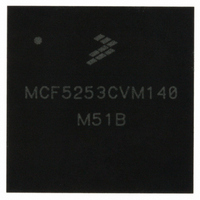
MCF5253CVM140 Freescale Semiconductor, MCF5253CVM140 Datasheet - Page 56

MCF5253CVM140
Manufacturer Part Number
MCF5253CVM140
Description
IC MPU 32BIT 140MHZ 225-MAPBGA
Manufacturer
Freescale Semiconductor
Series
MCF525xr
Datasheets
1.MCF5253VM140J.pdf
(34 pages)
2.MCF5253VM140J.pdf
(8 pages)
3.MCF5253VM140J.pdf
(648 pages)
4.MCF5253VM140J.pdf
(2 pages)
Specifications of MCF5253CVM140
Core Processor
Coldfire V2
Core Size
32-Bit
Speed
140MHz
Connectivity
CAN, EBI/EMI, I²C, QSPI, UART/USART, USB OTG
Peripherals
DMA, WDT
Program Memory Type
ROMless
Ram Size
128K x 8
Voltage - Supply (vcc/vdd)
1.08 V ~ 1.32 V
Data Converters
A/D 6x12b
Oscillator Type
External
Operating Temperature
-40°C ~ 85°C
Package / Case
225-MAPBGA
Family Name
MCF5xxx
Device Core
ColdFire V2
Device Core Size
32b
Frequency (max)
140MHz
Instruction Set Architecture
RISC
Supply Voltage 1 (typ)
1.2/3.3V
Operating Supply Voltage (max)
1.32/3.6V
Operating Supply Voltage (min)
1.08/3V
Operating Temp Range
-40C to 85C
Operating Temperature Classification
Industrial
Mounting
Surface Mount
Pin Count
225
Package Type
MA-BGA
Lead Free Status / RoHS Status
Lead free / RoHS Compliant
Number Of I /o
-
Eeprom Size
-
Program Memory Size
-
Lead Free Status / Rohs Status
Compliant
Available stocks
Company
Part Number
Manufacturer
Quantity
Price
Company:
Part Number:
MCF5253CVM140
Manufacturer:
FREESCALE
Quantity:
300
Company:
Part Number:
MCF5253CVM140
Manufacturer:
Freescale Semiconductor
Quantity:
10 000
Part Number:
MCF5253CVM140
Manufacturer:
FREESCALE
Quantity:
20 000
Company:
Part Number:
MCF5253CVM140J
Manufacturer:
Freescale Semiconductor
Quantity:
10 000
- MCF5253VM140J PDF datasheet
- MCF5253VM140J PDF datasheet #2
- MCF5253VM140J PDF datasheet #3
- MCF5253VM140J PDF datasheet #4
- Current page: 56 of 648
- Download datasheet (8Mb)
Signal Description
2.13
There is a 3-line subcode interface on the MCF5253. This 3-line subcode interface allows the device to
format and transmit subcode in EIAJ format to a CD channel encoder device. The three signals are
described in
2.14
The ADOUT signal on the ADOUT/SCLK4/GPIO58 pin provides the reference voltage in PWM format.
Therefore this output requires an external integrator circuit (resistor/capacitor) to convert it to a DC level
to be input to the ADREF pin.
The six AD inputs are each fed to their own comparator the reference input to each (ADREF) is then
multiplexed as only one AD comparison can be made at any one time.
2.15
The device has a versatile flash card interface that supports both SecureDigital and MemoryStick cards.
The interface can either support one SecureDigital or two MemoryStick cards. No mixing of card types is
possible.
2-10
RCK/QSPIDIN/QSPIDOUT/GPIO26 Subcode clock input. When pin is used as subcode clock, this pin is driven by the CD
Subcode Interface Signal
QSPIDOUT/SFSY/GPIO27
QSPICLK/SUBR/GPIO25
EBUIN3/CMD_SDIO2/GPIO14
EBUIN2/SCLKOUT/GPIO13
Table 2-9
Subcode Interface
Analog to Digital Converter (ADC)
Secure Digital / Memory Stick Card Interface
Flash Memory Signal
Table
To use the ADINx as General Purpose inputs (rather than the analog
function) it is necessary to generate a fixed comparator voltage level of
VDD/2. This is accomplished by a potential divider network connected to
the ADREF pin. However in portable applications where stand-by power
consumption is important, the current taken by the divider network (in
stand-by mode) can be excessive. Therefore it is possible to generate a
VDD/2 voltage by selecting SCLK4 output mode and feeding this clock
signal (which is 50% duty cycle) through an external integration circuit.
This generates a voltage level equal to VDD/2, however when stand-by
mode is selected it is disabled.
2-8.
gives the pin descriptions.
Subcode sync output. This signal is driven high if a subcode sync needs to be inserted in
Subcode data output. This signal is a subcode data out pin.
channel encoder.
the EFM stream.
Table 2-9. Flash Memory Card Signals
Table 2-8. Subcode Interface Signal
MCF5253 Reference Manual, Rev. 1
Clock out for both MemoryStick interfaces and for SecureDigital.
Secure Digital command line. MemoryStick interface 2 data I/O.
NOTE
Description
Description
Freescale Semiconductor
Related parts for MCF5253CVM140
Image
Part Number
Description
Manufacturer
Datasheet
Request
R
Part Number:
Description:
Mcf5253 Coldfire? Microprocessor Data Sheet
Manufacturer:
Freescale Semiconductor, Inc
Datasheet:
Part Number:
Description:
Manufacturer:
Freescale Semiconductor, Inc
Datasheet:
Part Number:
Description:
Manufacturer:
Freescale Semiconductor, Inc
Datasheet:
Part Number:
Description:
Manufacturer:
Freescale Semiconductor, Inc
Datasheet:
Part Number:
Description:
Manufacturer:
Freescale Semiconductor, Inc
Datasheet:
Part Number:
Description:
Manufacturer:
Freescale Semiconductor, Inc
Datasheet:
Part Number:
Description:
Manufacturer:
Freescale Semiconductor, Inc
Datasheet:
Part Number:
Description:
Manufacturer:
Freescale Semiconductor, Inc
Datasheet:
Part Number:
Description:
Manufacturer:
Freescale Semiconductor, Inc
Datasheet:
Part Number:
Description:
Manufacturer:
Freescale Semiconductor, Inc
Datasheet:
Part Number:
Description:
Manufacturer:
Freescale Semiconductor, Inc
Datasheet:
Part Number:
Description:
Manufacturer:
Freescale Semiconductor, Inc
Datasheet:
Part Number:
Description:
Manufacturer:
Freescale Semiconductor, Inc
Datasheet:
Part Number:
Description:
Manufacturer:
Freescale Semiconductor, Inc
Datasheet:
Part Number:
Description:
Manufacturer:
Freescale Semiconductor, Inc
Datasheet:


