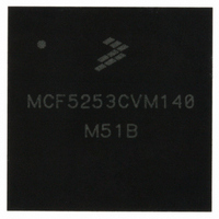
MCF5253CVM140 Freescale Semiconductor, MCF5253CVM140 Datasheet - Page 53

MCF5253CVM140
Manufacturer Part Number
MCF5253CVM140
Description
IC MPU 32BIT 140MHZ 225-MAPBGA
Manufacturer
Freescale Semiconductor
Series
MCF525xr
Datasheets
1.MCF5253VM140J.pdf
(34 pages)
2.MCF5253VM140J.pdf
(8 pages)
3.MCF5253VM140J.pdf
(648 pages)
4.MCF5253VM140J.pdf
(2 pages)
Specifications of MCF5253CVM140
Core Processor
Coldfire V2
Core Size
32-Bit
Speed
140MHz
Connectivity
CAN, EBI/EMI, I²C, QSPI, UART/USART, USB OTG
Peripherals
DMA, WDT
Program Memory Type
ROMless
Ram Size
128K x 8
Voltage - Supply (vcc/vdd)
1.08 V ~ 1.32 V
Data Converters
A/D 6x12b
Oscillator Type
External
Operating Temperature
-40°C ~ 85°C
Package / Case
225-MAPBGA
Family Name
MCF5xxx
Device Core
ColdFire V2
Device Core Size
32b
Frequency (max)
140MHz
Instruction Set Architecture
RISC
Supply Voltage 1 (typ)
1.2/3.3V
Operating Supply Voltage (max)
1.32/3.6V
Operating Supply Voltage (min)
1.08/3V
Operating Temp Range
-40C to 85C
Operating Temperature Classification
Industrial
Mounting
Surface Mount
Pin Count
225
Package Type
MA-BGA
Lead Free Status / RoHS Status
Lead free / RoHS Compliant
Number Of I /o
-
Eeprom Size
-
Program Memory Size
-
Lead Free Status / Rohs Status
Compliant
Available stocks
Company
Part Number
Manufacturer
Quantity
Price
Company:
Part Number:
MCF5253CVM140
Manufacturer:
FREESCALE
Quantity:
300
Company:
Part Number:
MCF5253CVM140
Manufacturer:
Freescale Semiconductor
Quantity:
10 000
Part Number:
MCF5253CVM140
Manufacturer:
FREESCALE
Quantity:
20 000
Company:
Part Number:
MCF5253CVM140J
Manufacturer:
Freescale Semiconductor
Quantity:
10 000
- MCF5253VM140J PDF datasheet
- MCF5253VM140J PDF datasheet #2
- MCF5253VM140J PDF datasheet #3
- MCF5253VM140J PDF datasheet #4
- Current page: 53 of 648
- Download datasheet (8Mb)
2.5
There are three chip select outputs on the MCF5253 device. CS0/CS4 and CS1/QSPI_CS3/GPIO28 and
CS2 which is associated with the IDE interface read and write strobes—IDE_DIOR and IDE_DIOW.
CS0 and CS4 are multiplexed. The MCF5253 has the option to boot from an internal Boot Rom.
The function of the CS0/CS4 pin is determined by the boot mode. When the device is booted from internal
ROM, the internal ROM is accessed with CS0 (required for boot) and the CS0/CS4 pin is driven by CS4.
When the device is booted from external ROM / Flash, the CS0/CS4 pin is driven by CS0 and the internal
ROM is disabled.
The active low chip selects can be used to access asynchronous memories. The interface is glueless.
2.6
The MCF5253 supports an ISA bus. Using the ISA bus protocol, reads and writes for one ISA bus
peripheral is possible. IDE_DIOR/GPIO31 and IDE_DIOW/GPIO32 are the read and write strobe. The
peripheral can insert wait states by pulling IDE_IORDY/GPIO33.
CS2 is associated with the IDE_DIOR and IDE_DIOW.
2.7
As the MCF5253 has a quite complicated slave bus, with the possibility of having DRAM, asynchronous
memories and an ISA peripherals on the bus, it may become necessary to introduce a buffer on the bus.
The MCF5253 has a glueless interface to steer these bus buffers with 2 bus buffer output signals
BUFENB1/GPIO29 and BUFENB2/GPIO30.
2.8
There are two I
The I
peripherals with an I
devices connected to the I
be accomplished with an open-drain output.
Freescale Semiconductor
Synchronous DRAM clock enable
2
C module acts as a two-wire, bidirectional serial interface between the MCF5253 processor and
Synchronous DRAM clock
Chip Selects
ISA Bus
Bus Buffer Signals
I
2
SDRAM Signal
C Module Signals
2
C interfaces on this device.
2
C interface (e.g., LED controller, A-to-D converter, D-to-A converter). When
2
C bus drive the bus, they will either drive logic-0 or high-impedance. This can
Table 2-2. SDRAM Controller Signals
The DRAM clock is driven by the BCLK/GPIO40 signal.
The BCLKE active high output signal is used during synchronous mode to route
directly to the SCKE signal of external SDRAMs. This signal provides the clock
enable to the SDRAM.
MCF5253 Reference Manual, Rev. 1
Description
Signal Description
2-7
Related parts for MCF5253CVM140
Image
Part Number
Description
Manufacturer
Datasheet
Request
R
Part Number:
Description:
Mcf5253 Coldfire? Microprocessor Data Sheet
Manufacturer:
Freescale Semiconductor, Inc
Datasheet:
Part Number:
Description:
Manufacturer:
Freescale Semiconductor, Inc
Datasheet:
Part Number:
Description:
Manufacturer:
Freescale Semiconductor, Inc
Datasheet:
Part Number:
Description:
Manufacturer:
Freescale Semiconductor, Inc
Datasheet:
Part Number:
Description:
Manufacturer:
Freescale Semiconductor, Inc
Datasheet:
Part Number:
Description:
Manufacturer:
Freescale Semiconductor, Inc
Datasheet:
Part Number:
Description:
Manufacturer:
Freescale Semiconductor, Inc
Datasheet:
Part Number:
Description:
Manufacturer:
Freescale Semiconductor, Inc
Datasheet:
Part Number:
Description:
Manufacturer:
Freescale Semiconductor, Inc
Datasheet:
Part Number:
Description:
Manufacturer:
Freescale Semiconductor, Inc
Datasheet:
Part Number:
Description:
Manufacturer:
Freescale Semiconductor, Inc
Datasheet:
Part Number:
Description:
Manufacturer:
Freescale Semiconductor, Inc
Datasheet:
Part Number:
Description:
Manufacturer:
Freescale Semiconductor, Inc
Datasheet:
Part Number:
Description:
Manufacturer:
Freescale Semiconductor, Inc
Datasheet:
Part Number:
Description:
Manufacturer:
Freescale Semiconductor, Inc
Datasheet:


